Understanding ESD Damage: Types, Causes, and Impact on Component Reliability
Catastrophic, Latent, and Parametric Failure Modes
When it comes to electronics, electrostatic discharge or ESD can really mess with component reliability in three main ways. First there's what we call catastrophic failures where something gets hit by those high voltage spikes and just stops working completely right away. Then there are these sneaky latent failures that don't show up until much later. Components might pass all the tests at first glance, but inside they start degrading slowly over time. This becomes a big problem down the road when devices fail unexpectedly in important places like hospitals, airplanes, or cars. The third type is parametric failures which change how things work electrically without actually breaking them. Think stuff like higher leakage currents or different voltage levels that gradually make components perform worse than they should. According to recent numbers from the EOS/ESD Association back in 2023, about one third of all semiconductor failures during manufacturing are caused by ESD problems. And when this happens in advanced integrated circuit production, companies can end up losing hundreds of thousands of dollars per incident.
Physical Degradation: Gate Oxide Rupture, Dielectric Breakdown, and Junction Damage
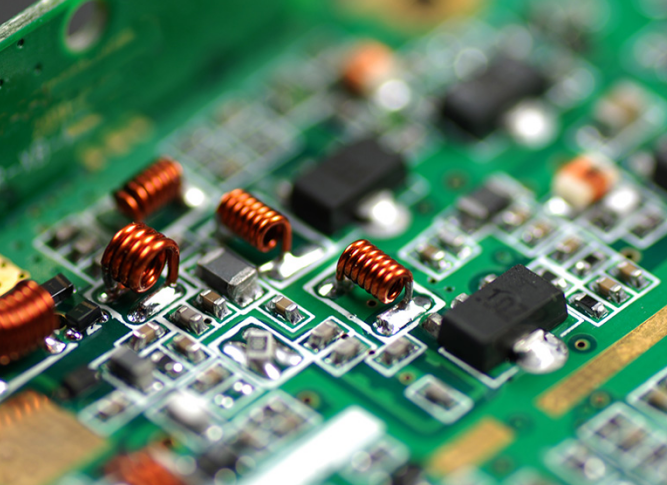
Looking at things under a microscope, electrostatic discharge causes structural problems in three main ways. When it comes to MOSFETs, what happens is called gate oxide rupture. Basically, the discharge punches through those super thin insulation layers. This becomes a bigger problem as technology gets smaller than 10 nanometers because these oxide layers are sometimes only around 5 to 10 atoms thick. Then there's dielectric breakdown which basically means creating unwanted conductive paths inside capacitors or other insulators, usually leading to short circuits. Another issue is junction damage caused by heat stress. The intense heat melts the connections between silicon and metal parts, changing how transistors work forever. Most of these failures start with regular old human contact. Just walking on carpet can build up about 1.5 kilovolts of charge. Other culprits include bad tools or dirt that makes surfaces conduct electricity too easily. How vulnerable something is depends a lot on what kind of device we're talking about.
- Low-voltage ICs: Fail at <100 V
- Discrete diodes: Typically withstand 2–5 kV
- Advanced processors: Can be damaged by discharges below 250 V
ESD Protection Strategies: From On-Chip Design to System-Level Implementation
Effective ESD protection requires a coordinated, multi-layered approach—integrating safeguards directly into silicon while reinforcing them at the board and system levels. This defense-in-depth strategy ensures transient threats are intercepted before reaching sensitive circuitry.
Integrated On-Chip ESD Protection: Diodes, SCRs, and Snapback Devices
On-chip protection structures are fabricated directly into integrated circuits to intercept ESD events at the pin level. Key solutions include:
- Clamp diodes: Divert transient currents to power rails or ground once voltage exceeds safe thresholds
- SCRs (Silicon Controlled Rectifiers): Activate low-impedance conduction paths during high-current events via controlled latch-up
- Snapback devices: Leverage NMOS/PMOS configurations that transition to lower-voltage, high-current states after triggering
These nanosecond-response elements limit voltage overshoot to less than 10% of destructive levels—critical for preserving gate oxides and junction integrity. Designers must carefully balance protection strength against parasitic capacitance, particularly in high-speed interfaces (e.g., PCIe 6.0, USB4), where excess capacitance can distort signal integrity above 5 Gbps.
System-Level ESD Protection: TVS Diodes, Filtering, and PCB Layout for Robustness
Board-level protection complements on-chip defenses by managing higher-energy transients that exceed semiconductor tolerances. Essential elements include:
- TVS (Transient Voltage Suppression) diodes: Placed within 2 mm of I/O connectors to clamp voltages below 5 V in under 1 ns
- Π-filters: Combine ferrite beads and decoupling capacitors to attenuate high-frequency ESD noise (>100 MHz)
-
PCB layout best practices:
- Continuous, low-impedance ground planes (<15 mΩ)
- Minimal trace length between TVS devices and protected ICs
- Strategic separation of analog, digital, and RF sections to prevent coupling
When implemented per IEC 61000-4-2 guidelines, these measures can elevate system-level ESD immunity by 4–8 kV. The most robust designs integrate TVS clamping with optimized routing to establish predictable, low-impedance discharge paths—steering energy away from sensitive nodes.
ESD Protective Packaging and Handling for Component Integrity
Keeping components intact throughout the entire process from wafer fabrication all the way to final use requires strict control over how they’re packaged and handled. There are several key materials used for this purpose. Static dissipative bags help get rid of surface charges because they have resistance levels between 10^4 and 10^11 ohms. Conductive trays made with carbon loaded polymers actually conduct away any stray electrical currents. And then there are those fancy metallized containers that create multiple layers of protection against outside electrostatic fields. When moving parts around, special component holders keep everything in place so nothing gets damaged during transit. Logistics operations also benefit from ESD safe pallets which prevent that annoying triboelectric effect where things build up static electricity just by rubbing together.
The key things people need to follow when handling sensitive components are things like making sure staff members are grounded using those wrist straps that get tested every day, having ionizers placed around work surfaces to knock out any leftover static charge, and putting those standard warning signs everywhere - usually those yellow triangles on packages that everyone knows what they mean. All together, this setup keeps the static electricity levels down under 100 volts. Industry research shows that keeping it at this level cuts down on something called parametric drift, which is basically the first sign that there might be hidden ESD damage happening. Studies indicate this approach can cut such issues by more than 30 percent according to various reports from manufacturing sectors.