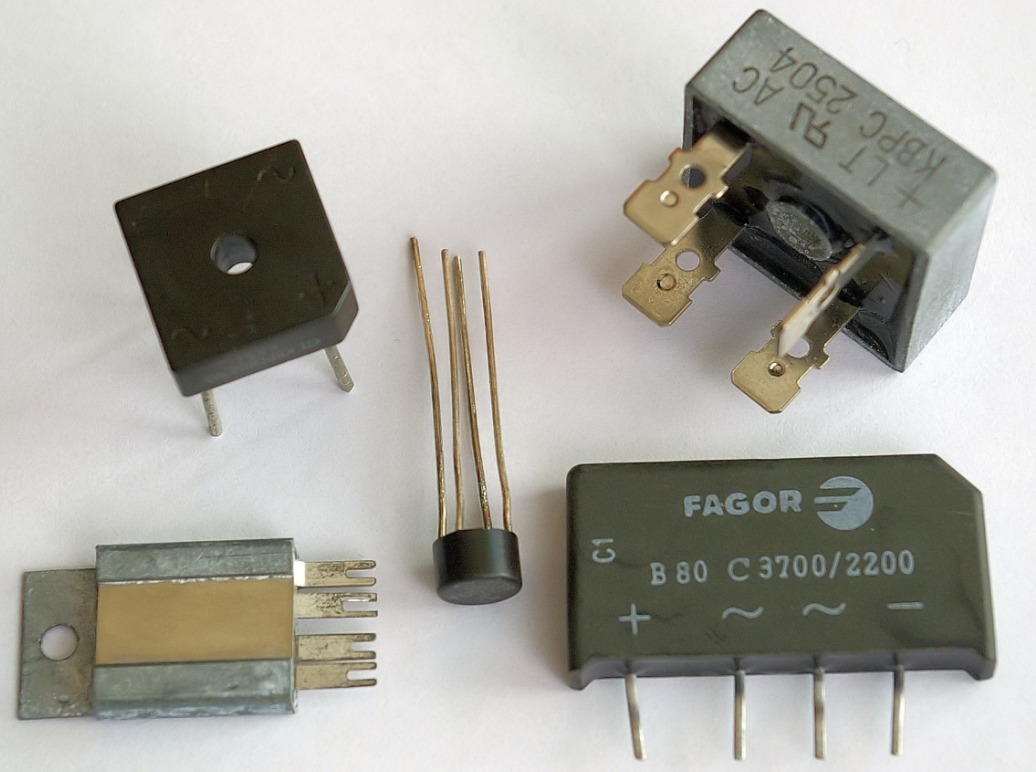
Core Electrical Ratings: VRMS, VRRM, IF(AV), and IO Explained
Why Peak Inverse Voltage (VRRM) Must Exceed AC Input Peaks & Not Just VRMS
Choosing a bridge rectifier just by looking at RMS voltage (VRMS) is asking for trouble down the road. The reality is that AC power lines actually reach much higher voltages than what's measured as RMS. Take standard 120V power for instance it hits around 170V at its peak because of how AC works mathematically (√2 times VRMS). What matters most here is something called VRRM, which tells us how much reverse voltage those little diodes inside can handle before they give out completely. When this rating falls below what the actual incoming voltage might hit, all sorts of problems pop up from unexpected power spikes or electrical noise bouncing back through circuits. Most experienced engineers will tell you to go with components rated at least 1.5 times higher than these peak values so there's some breathing room for unpredictable conditions. For regular household 120V setups, that means aiming for ratings above 255 volts according to international safety standards like IEC 62368-1.
Derating IF(AV) and IO for Duty Cycle, Ambient Temperature, and Transient Loads
Average forward current (IF(AV)) and surge current (IO) ratings assume ideal lab conditions: 25°C ambient and steady-state loads. Real-world operation demands rigorous derating:
- Temperature: Junction temperature rise directly reduces current capacity; at 100°C ambient, IF(AV) may drop by 40% versus datasheet specs.
- Duty cycle: Intermittent high-current events—like motor startups—require validation against IO’s pulse-width and repetition-rate limits.
-
Transients: Capacitor inrush currents often exceed IO; mitigate with NTC thermistors or series current-limiting resistors.
Always cross-reference thermal derating curves and transient pulse ratings— not just headline values— to ensure reliability across your operating envelope.
Thermal Performance and Real-World Cooling Requirements
Junction-to-Ambient Resistance (RθJA) vs. Actual PCB Layout: Copper Area, Trace Width, and Thermal Vias
Datasheet RθJA values assume idealized test conditions—typically a large copper pad on a single-layer board with forced airflow. In practice, thermal performance is dictated by PCB implementation:
- Doubling copper pour area beneath the rectifier can reduce junction temperature by 15–20°C.
- Narrow traces act as thermal bottlenecks; ≥1.5 mm trace width is recommended for high-current paths.
- Thermal vias placed under the package (≥8 vias/cm², filled or plated) cut thermal resistance by up to 40% by transferring heat to inner layers or ground planes.
Forced-air cooling becomes necessary above 50°C ambient, as every 10°C rise beyond rated limits halves component lifetime (per Arrhenius model). Enclosed enclosures or high-altitude deployments require 30–50% power derating due to reduced convection efficiency. Validate designs using thermal simulation tools—prioritizing ≥2 oz copper weight, optimized via density, and low-thermal-resistance heatsink interfaces— to avoid premature failure masked by optimistic RθJA figures.
Bridge Rectifier Data Sheet Pitfalls to Avoid
The 'Typical' Forward Voltage Fallacy: Why VF at High IF Causes Unexpected Losses and Heating
Most datasheets highlight what they call "typical" forward voltage (VF) measurements taken at 25°C using very low test currents. What this approach hides is how dramatically VF actually changes with different load currents and temperatures. When components operate at their maximum rated current (IF), the forward voltage often jumps anywhere from 0.2 to 0.4 volts above what's listed in specifications. This small increase leads to significantly higher conduction losses, sometimes as much as 20% to 30%. Take for instance a 0.2 volt rise at 5 amps - that creates an extra watt of heat that wasn't accounted for in design calculations. Designers then have to either reduce component ratings or implement additional cooling solutions. While top manufacturers do test VF under pulsed conditions that better match real world switching scenarios, many engineers still stick exclusively to those static spec sheets measured at room temperature. This mismatch creates serious problems down the line, especially when heatsinks turn out to be inadequate for the actual power dissipation during peak loads.
Ignoring Reverse Recovery Time (trr) in High-Frequency SMPS & Impact on EMI and Efficiency
The reverse recovery time (trr) has a major impact on both switching losses and electromagnetic interference (EMI) in switch-mode power supplies (SMPS). When standard rectifiers have trr values over 500 nanoseconds, they create noticeable current ringing when turning off. This ringing activates parasitic LC circuits and generates broad spectrum EMI at frequencies that are multiples of the main switching frequency. According to recent research from the IEEE EMC Society published last year, these effects can boost system noise levels between 12 to almost 18 decibels while reducing overall efficiency somewhere around 3% to 8% because of energy losses during regeneration. For modern SMPS designs running above 100 kilohertz, engineers need ultra fast diodes with trr below 100 nanoseconds. Unfortunately, many component specifications still don't include information about how trr changes with temperature or forward current. This missing data is particularly problematic for small form factor power supplies where heat buildup becomes an issue, since higher die temperatures tend to make recovery characteristics worse anyway.
System-Level Integration: Filtering, Layout, and Reliability Synergy
A bridge rectifier’s performance extends far beyond its datasheet specifications. Effective integration hinges on harmonizing filtering, physical layout, and thermal pathways to ensure stability under real-world stresses. Key considerations include:
-
Filtering Synergy: AC ripple attenuation depends not just on bulk capacitance, but on capacitor type (low-ESR electrolytic or polymer), placement proximity to the rectifier, and impedance matching to the rectifier’s dynamic impedance profile. Poorly implemented filtering elevates downstream regulator stress and amplifies conducted EMI.
-
Layout-Driven Reliability: Minimizing the AC loop area formed by the transformer secondary, rectifier inputs, and bulk capacitor suppresses inductive voltage spikes that threaten diode integrity. Strategic copper pour under the rectifier and dense thermal vias lower effective θJA, while proper spacing between high-dv/dt nodes mitigates capacitive coupling noise.
-
Thermal-Electrical Coupling: Elevated die temperature increases VF, raising conduction losses— which in turn generate more heat. This positive feedback loop accelerates degradation and risks thermal runaway. Cooling solutions must account for ambient temperature rise, adjacent heat sources, and long-term aging effects— not just instantaneous power dissipation.
Ignoring these interdependencies risks premature failure, even with a robust bridge rectifier. Proactive design— grounded in verified filtering efficacy, low-inductance routing, and thermally validated layouts— transforms a standalone component into a resilient, field-proven power conversion stage.