Explore the working principle, equivalent circuit, key parameters, and selection tips for ESD protection diodes. Designed for USB, HDMI, and power input interface protection, capable of suppressing ±8kV ESD surges per IEC 61000-4-2 to ensure system reliability.
Electrostatic Discharge (ESD) is a phenomenon in which electrical charge is released in a short period of time due to a potential difference between charged objects. It can cause irreversible damage to precision electronic devices. As electronic devices continue to evolve toward higher speed and miniaturization, the requirements for ESD protection have become more stringent. ESD protection diodes, as efficient and reliable protective components, are widely used at critical points such as signal interfaces and power inputs.
1. Basic Working Principle of ESD Protection Diodes
ESD protection diodes are typically composed of a reverse-biased PN junction. Their core mechanism utilizes the breakdown characteristics of the diode to quickly conduct and divert overcurrent to ground when a high voltage, such as an ESD surge, is applied externally. This prevents damage to downstream components.
Normal Operation: When the signal line voltage (VIN) is within the range of 0 to the Maximum Reverse Working Voltage (VRWM), the diode remains off and behaves like a junction capacitance (CT).
Overvoltage Conduction: When the voltage exceeds the Breakdown Voltage (VZ), the diode enters reverse breakdown mode, conducts current, and clamps the voltage to a certain level (VC) to protect the load.
In the conduction state, the ESD protection diode can be modeled as a series connection of a clamping voltage source and a dynamic resistance (RDYN). Its clamping performance is closely related to its internal structure.
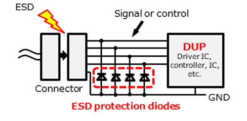
(Illustration: Example of ESD Protection Diode Connection)
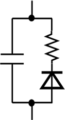
(Illustration: Equivalent Circuit of ESD Protection Diode)
2. Analysis of Key Electrical Parameters
VRWM (Maximum Reverse Working Voltage): The highest reverse voltage at which the device can operate without conducting.
VZ (Breakdown Voltage): The minimum voltage at which the device begins to conduct in reverse, determining its response threshold.
VC (Clamping Voltage): The voltage across the device during conduction at a specified current, which directly reflects the strength of the protection.
RDYN (Dynamic Resistance): The internal resistance during conduction, affecting the voltage drop. Lower values are preferred.
CT (Junction Capacitance): The parasitic capacitance exhibited in the off state, which affects high-speed signal integrity and should be minimized.
3. Equivalent Circuit Models in Operation
ESD diodes have two typical states of operation:
During normal conditions, the device behaves like a small capacitor, mainly affecting high-frequency performance.
When an ESD surge occurs, the diode rapidly switches to conduction mode, forming a clamping path composed of an equivalent series resistance and voltage source.
In practice, ESD voltage has a very steep rising edge (<1 ns). At this time, the parasitic inductance and capacitance of PCB traces can also affect protection effectiveness. Therefore, layout optimization is necessary.
4. Analysis of ESD Surge Response
Assume an 8kV ESD event is applied to an interface. According to IEC 61000-4-2, the surge current can reach up to 30A. If the diode has a dynamic resistance of 0.5Ω, the transient voltage drop will be 15V, which is added to the clamping voltage. Therefore, selecting devices with low RDYN and low VC is important to reduce the total clamping voltage and minimize electrical stress on the protected device (DUP).
5. Application Layout and Selection Recommendations
In ESD protection design, in addition to the parameters of the device itself, PCB layout plays a crucial role. The following principles should be followed:
Place ESD protection devices as close to external connectors as possible to reduce parasitic inductance and capacitance in traces.
Connect the ground pins directly to a large ground plane to avoid inductive loops.
For high-frequency interfaces such as USB 3.0 or HDMI, low capacitance models (e.g., CT ≤ 0.5pF) are recommended.
For multi-channel protection, consider using TVS arrays or integrated protection modules.
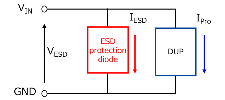
(Illustration: Simple Circuit Configuration During ESD Surge)
6. Overview of ESD Test Standards
Common ESD immunity test standards include:
IEC 61000-4-2: System-level ESD immunity testing standard simulating the human body discharge model; typical test levels include ±4kV and ±8kV.
JEDEC JESD22-A114: Human Body Model (HBM) testing standard at the chip level.
MIL-STD-883: Military standard for evaluating ESD resistance of components.
ANSI/ESD S20.20: Standard for establishing ESD control systems, covering production processes and environmental control.
7. Conclusion
ESD protection diodes play an indispensable role in modern electronic product design by rapidly responding to ESD events and clamping transient voltages. When selecting ESD protection devices, one should consider response speed, clamping voltage, dynamic resistance, and junction capacitance. Proper deployment and PCB layout based on the specific system interfaces are also key to achieving optimal protection performance.