Understanding ESD: How Electrostatic Discharge Damages Sensitive Electronics
The Physics of ESD: Gate Oxide Rupture and Latch-Up in CMOS ICs
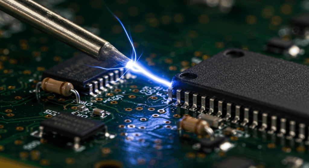
ESD happens when static electricity builds up and then jumps between objects with different electrical charges. What makes it dangerous? Well, those sudden voltage surges measure in the thousands but we can't see them at all. For CMOS chips, this energy goes after the weakest spots first. High voltage spikes tear through those super thin gate oxide layers, which basically kills the transistors right away. There's another problem too. Those pesky parasitic silicon controlled rectifiers hidden in the chip substrate might activate during an ESD event. When they do, they create these low resistance paths that let destructive currents flow freely, sometimes reaching several amps worth of power. Modern integrated circuits are getting smaller and work at much lower voltages now, down to around 1.2 volts in some cases. Even something as small as 100 volts, way below what our senses can detect, could wreck a chip completely. Thermal models show that brief current spikes over 10 amps can actually melt the tiny connections inside a chip in less than half a billionth of a second. That's why proper ESD protection isn't just nice to have anymore it's absolutely essential for keeping electronics from failing catastrophically.
Types of ESD Damage: Catastrophic, Latent, and Parametric Failures
Electrostatic discharge shows up in three main ways when it comes to damaging electronics, and these problems get progressively worse as devices age. The most obvious type is catastrophic failure where the device basically dies right away from visible damage like burnt parts or melted metal paths that can be seen during testing. Then there's latent damage which is much sneakier. Tiny holes form in semiconductor connections or gate oxides break down over time. These issues might pass initial tests but eventually cause products to fail early in the field. Industry reports suggest that boards with hidden ESD damage often last only 40 to 60 percent as long as they should. Parametric failures are another category where electrical properties change without complete failure. Think increased leakage current or voltage levels shifting out of spec, which messes with timing and signal quality. Fixing catastrophic failures typically costs around $5,000 each according to Ponemon research from 2023, while dealing with latent issues eats into warranty budgets because figuring out what went wrong takes so much time and effort. Good ESD protection needs to cover all these scenarios with multiple layers of defense throughout the manufacturing process.
| Failure Type | Detection Window | Financial Impact | Physical Manifestation |
|---|---|---|---|
| Catastrophic | Immediate | Scrap + production halt | Melted interconnects, oxide rupture |
| Latent | Weeks to months | Warranty claims + recalls | Progressive junction degradation |
| Parametric | During testing | Yield loss + rework | Elevated leakage, timing drift |
Core ESD Protection Mechanisms and Component Solutions
How TVS Diodes and Surge Suppressors Divert ESD Energy
TVS diodes act as the primary defense mechanism against electrical surges by directing excess current away from delicate circuitry when something like an 8kV static discharge occurs from a human body model test. What makes these components effective is their ability to rapidly clamp down on voltage spikes thanks to a process called low impedance avalanche breakdown. They can handle surges as high as 30 amps before sending them safely to ground, all while keeping downstream circuits operating within acceptable limits. Response times are incredibly fast too, often below one nanosecond which explains why they work so well with modern high speed connections such as those found in USB 3.0 ports or HDMI cables. For situations involving even larger energy bursts, multi layer varistors come into play. These offer additional protection against transients exceeding 20kV through a different mechanism where electrons scatter across metal oxide materials inside the device. Because of this capability, they find common use in protecting power supply lines within various industrial settings where extreme conditions might otherwise cause damage.
Clamping Voltage, Response Time, and TLP Characterization in Real-World Applications
When it comes to protecting against electrostatic discharge, there are basically three things that matter most: how much voltage gets clamped, how fast the device reacts, and what happens when we test it with Transmission Line Pulses (TLP). Take a TVS diode rated at 5 volts for clamping - this keeps those sensitive integrated circuits safe since their gate oxide tends to break down around 10 volts. For RF stuff like 5G antennas, getting response times under half a nanosecond really makes a difference. Otherwise, tiny bits of damage can build up over time without anyone noticing. Testing with TLP methods according to IEC 61000-4-2 standards shows us exactly how these devices fail. Looking at current versus voltage plots helps engineers tell if something snaps back suddenly or clamps gently. What manufacturers find is that good TVS diodes hold their dynamic resistance below 10 ohms even during big 30 amp pulses. This actually beats out polymer based solutions when dealing with high frequency signals in modern electronics.
Comparing ESD Suppression Technologies
| Component | Typical Clamping Voltage | Response Time | Max Surge Current | Use Case |
|---|---|---|---|---|
| TVS Diode | 3–15V | <1 ns | 30A | High-speed data lines |
| Multi-layer Varistor | 20–600V | 5–50 ns | 70A | Power supply rails |
| Gas Discharge Tube | 75–1000V | 100–500 ns | 20kA | Telecom infrastructure |
Balancing clamping precision and surge capacity is essential–over-engineering increases cost, while under-protection risks CMOS latch-up.
Designing Effective ESD Protection Circuits for Modern Electronics
To design good ESD protection circuits, it's important to place those suppression components such as TVS diodes right next to connectors and input/output ports where surges tend to enter first before reaching the delicate integrated circuits. The clamping voltage needs to be set just below what would damage the components being protected. At the same time, keeping junction capacitance low helps maintain signal quality for those fast data transfers we see in modern interfaces. Shorter paths on the PCB board reduce trace inductance which makes the whole system respond better when needed. Many engineers now prefer multi stage protection setups because they handle tough situations much better than single point solutions. Following standards like ANSI/ESD S20.20-2021 gives manufacturers peace of mind knowing their products can withstand both sudden failures and slow wearing away over time. This matters even more today since chips are getting smaller all the time, down into nanometer sizes where they actually become more vulnerable to electrostatic damage. Testing at the system level with TLP methods is still crucial though, as lab results don't always match what happens out there in the field with all sorts of unexpected static events.
ESD-Safe Work Environments: From Workstations to Packaging
Static-Dissipative Flooring and ISO 6360 Compliance in Manufacturing
Creating an ESD safe environment starts with proper flooring materials like EPDM tiles infused with conductive properties. These floors keep their surface resistance within the range of 1 million to 1 billion ohms, allowing static charges to dissipate safely rather than accumulate. According to ISO 6360-5 standards, facilities need to test their floor resistance and grounding connections regularly. Companies following these guidelines have seen around 75% fewer electrostatic discharge incidents than those that don't comply, according to research from ERAI in 2023. The system works by bonding grounding points between the floor, work surfaces, and actual earth ground. This creates a complete circuit that stops voltage from building up beyond 100 volts, which is generally considered the safety threshold for delicate integrated circuits used in electronics manufacturing.
Dual-Layer Shielding Bags and Faraday Cage Principles for Safe Storage
Shielding bags with two layers work based on Faraday cage concepts to keep components safe when stored or moved around. The outside layer has metal coating that pushes away any static electricity from outside sources, while the inside part made of special plastic helps get rid of built-up charges within the bag itself. These protective bags cut down electrostatic energy levels by about 50 decibels, stopping discharges over roughly 8,000 volts according to IEC standards. Getting the seal right matters a lot actually because if it's not closed properly, the protection drops by almost 90 percent. When dealing with sensitive stuff like CMOS sensors, putting them in controlled environment cabinets where humidity stays below thirty percent really helps prevent hidden problems later on. Keeping that Faraday shield intact all through shipping and handling remains super important since even one moment without proper protection can undo everything else done to safeguard those valuable parts.
Frequently Asked Questions
What is electrostatic discharge (ESD)?
Electrostatic discharge (ESD) occurs when there is a sudden flow of electricity between two electrically charged objects, often causing damage to sensitive electronics.
Why is ESD protection important for electronics?
ESD protection is crucial because electrostatic discharge can cause catastrophic failures, latent damage, and parametric changes in electronic components, leading to shortened lifespan and high repair costs.
How does ESD damage electronics?
ESD can rupture gate oxides and activate parasitic silicon controlled rectifiers in CMOS ICs, causing destructive currents that damage the device.
What are TVS diodes?
TVS diodes are protective components used to divert excess current and voltage surges away from delicate circuitry, preventing damage from electrostatic discharge.
What is a Faraday cage, and how does it protect electronics?
A Faraday cage is a structure that shields its contents from static and electromagnetic fields, often used as a packaging solution for storing electronic components safely.