این پی این ٹرانزسٹرز کی ساخت اور تشکیل کو سمجھنا
سیلیکون کی بنیاد پر تعمیر اور این پی این جنکشن کی تہہ دار ساخت
این پی این ٹرانزسٹر کا دل نائیٹروجن ٹائپ اور پی ٹائپ سلیکان کو احتیاط سے ڈوپنگ کے عمل کے ذریعے ملانے میں پوشیدہ ہوتا ہے۔ ہم اس کی تعمیر کو سمجھتے ہیں: عموماً ایک زیادہ ڈوپ شدہ این ٹائپ علاقہ ایمیٹر کے طور پر کام کرتا ہے، اس کے بعد بیس کے لیے ہلکے ڈوپ شدہ پی ٹائپ میٹریل کی ایک پتلی پرت ہوتی ہے، اور آخر میں ایک اور این ٹائپ حصہ (معتدل ڈوپ شدہ) کلیکٹر کے طور پر کام کرتا ہے۔ یہ ترتیب ان ضروری پی این جنکشنز کو وجود میں لاتی ہے جو کنٹرول کرتی ہیں کہ الیکٹرانز کیسے حرکت کرتے ہیں۔ جب ان اجزاء کے ساتھ کام کیا جاتا ہے، تو تیار کرنے والے زیادہ خالص سلیکان کو ترجیح دیتے ہیں کیونکہ یہ کرسٹل لیٹس کی سالمیت کو برقرار رکھتا ہے اور چارجز کو کارآمد انداز میں حرکت کرنے دیتا ہے۔ جسمانی شکل کا معاملہ بھی اہمیت رکھتا ہے - مناسب جیومیٹری گرمی کے بوجھ کو سنبھالنے میں مدد کرتی ہے تاکہ ٹرانزسٹر لمبے عرصے تک لوڈ کنڈیشن کے تحت چلنے پر خراب یا ناکام نہ ہو۔
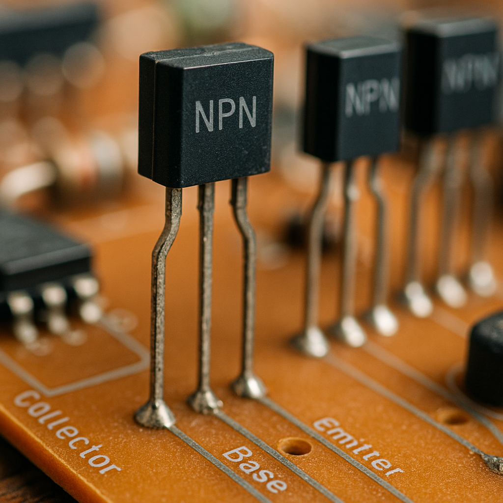
ایمیٹر، بیس، اور کلیکٹر علاقوں میں ڈوپنگ کے خاکے
ہم سیمی کنڈکٹر ڈیوائس کے مختلف حصوں میں ڈوپنگ کی سطح کو کس طرح ایڈجسٹ کرتے ہیں، یہی ان کی کارکردگی میں فرق ڈالتا ہے۔ مثال کے طور پر ایمیٹر علاقہ، اسے ڈوپنٹس کی ایک بھاری خوراک ملتی ہے، تقریبا 10 کی پاور 19 ایٹمز فی کیوبک سینٹی میٹر، جس سے ہمیں بہت سارے فری الیکٹرانز کو تیرتے ہوئے ملتے ہیں۔ بیس علاقے کو بہت کم ڈوپنگ کی ضرورت ہوتی ہے، کچھ اس طرح 10 کی 17 ویں پاور، تاکہ کیریئرز اپنے کام سے پہلے صرف غائب نہ ہو جائیں۔ اور پھر کلیکٹر میں ہم زیادہ اور کم ڈوپنگ کے درمیان ایک درمیانی راستہ اپناتے ہیں تاکہ وولٹیج سٹریس کے تحت چیزوں کو ٹوٹنے سے روکا جا سکے اور کرنٹ کے بہاؤ کو کارآمد بنایا جا سکے۔ جب مینوفیکچررز سلیکون ویفر میں فاسفورس اور بورون کو امپلانٹ کرتے ہیں، تو وہ بنیادی طور پر ان این ٹائپ اور پی ٹائپ زونز کو تخلیق کر رہے ہوتے ہیں جو ٹرانزسٹرز کو قابل اعتماد بناتے ہیں، اس بات کو کنٹرول کرتے ہوئے کہ آپریشن کے دوران الیکٹرانز کہاں سے جاتے ہیں اور کہاں سے آتے ہیں۔
- ایمیٹر : زیادہ الیکٹران کی تعداد = 10¹⁹/cm³
- Base : کم سے کم موٹائی = 1–2 μm، کم ڈوپنگ
- کولیکٹر : بریک ڈاؤن وولٹیج اور کرنٹ ہینڈلنگ کے لیے آپٹیمائیزڈ
ٹرانزسٹر کی جُھری سائز اور حرارتی کارکردگی کی ترقی
1960ء کی دہائی کے بعد سے ٹرانزسٹر کو چھوٹا کرنے کا عمل تقریباً مور کے قانون پر ہی چل رہا ہے، اس کے اجزاء کا سائز ملی میٹر سے نینو میٹر تک کم ہو چکا ہے۔ موجودہ 5nm پروسیس ایک مربع ملی میٹر کے اندر تقریباً 100 ملین NPN ٹرانزسٹرز رکھ سکتی ہے۔ چیزوں کو چھوٹا کرنے کے معاملے میں ہم نے بھی کافی پیش رفت دیکھی ہے۔ تانبے کے انٹرکنیکٹس کا مزاحمت اب 0.2 اوہم سے کم ہے، اور سلنگ سلیکان کے نام سے ایک ایسی چیز بھی موجود ہے جو الیکٹرانز کو تقریباً 35 فیصد تیزی سے حرکت کرنے دیتی ہے۔ حرارت کے مسائل کا سامنا کرنے کے لیے، انجینئرز نے ہیرے جیسی کاربن میٹریل کو حرارت کو پھیلانے کے لیے اور مائیکروفلوڈک کولنگ سسٹمز تک استعمال کیا ہے۔ یہ ایجادیں چپس کو 100 واٹ فی مربع سینٹی میٹر سے زیادہ پاور ڈینسٹی کو برداشت کرنے کی اجازت دیتی ہیں، بغیر 150 ڈگری سینٹی گریڈ سے زیادہ درجہ حرارت کو پہنچے، جو کہ سوچنے میں آنے والی بات ہے۔
این پی این ٹرانزسٹرز کیسے کام کرتے ہیں: بائس، کیریئر فلو، اور کرنٹ ایمپلیفیکیشن
بیس ایمیٹر اور بیس کلیکٹر جنکشن میں فارورڈ اور ریورس بائس
مناسب آپریشن کے لیے مخصوص بائس درکار ہے: بیس ایمیٹر جنکشن فارورڈ بائسڈ ہے (عموماً 0.6–0.7V پر) تاکہ کرنٹ فلو کی اجازت دی جا سکے، جبکہ بیس کلیکٹر جنکشن ریورس بائسڈ رہتا ہے۔ یہ کانفیگریشن ٹرانزسٹر کو ایکٹیو علاقے میں کام کرنے کی اجازت دیتی ہے، جہاں چھوٹی بیس کرنٹس بہت بڑی کلیکٹر کرنٹس کو کنٹرول کرتی ہیں—جس کی بنیاد ایمپلیفیکیشن پر ہوتی ہے۔
این پی این آپریشن میں الیکٹران انجریکشن اور ہولز کی دباؤ
بیس ایمیٹر جنکشن کو فارورڈ بائس کرنا ایمیٹر سے پی ٹائپ بیس میں الیکٹرانز کو داخل کر دیتا ہے۔ بیس کی تنگ چوڑائی—عموماً 1–2 مائیکرو میٹر—ریکمبینیشن کو کم کر دیتا ہے، یہ یقینی بناتے ہوئے کہ 90% سے زیادہ الیکٹران کلیکٹر تک پہنچ جائیں۔ اینالاگ ایپلی کیشنز میں زیادہ کرنٹ گین اور کم سگنل ڈسٹورشن کے لیے کیریئر ٹرانسپورٹ کی کارکردگی ناگزیر ہے۔
کرنٹ ایمپلیفیکیشن کا مکینزم: بیس کرنٹ سے کلیکٹر کرنٹ تک
تقویت کو β (بیٹا) کے ذریعے مقدار میں ظاہر کیا جاتا ہے، جہاں کلیکٹر کرنٹ IC = β × IB۔ معیاری اقسام β کی قدر 100 یا اس سے زیادہ فراہم کرتی ہیں، جبکہ ایکٹیو موڈ میں کلیکٹر کی کارکردگی 95 فیصد سے زیادہ ہوتی ہے۔ یہ اعلیٰ گین (gain) NPN ٹرانزسٹرز کو کم امپٹ کرنٹ کے ساتھ بڑے لوڈز کو چلانے کی اجازت دیتی ہے، جس کی وجہ سے انہیں تقویت اور سوئچنگ دونوں کے لیے موزوں بنایا جاتا ہے۔
سکیم میں الیکٹران کے بہاؤ اور روایتی کرنٹ کے فرق کو واضح کرنا
اگرچہ الیکٹران فزیکلی ایمیٹر سے کلیکٹر تک جاتے ہیں، لیکن سرکٹ کی تعمیر اور تجزیہ روایتی کرنٹ فلو (مسکین سے منفی) کے مطابق ہوتا ہے، جو 18 ویں صدی میں قائم کیا گیا تھا۔ انجینئرز اور تکنیکی کارکنان کو دونوں ماڈلز کو سمجھنا ضروری ہے: سکیم کی تشریح کے لیے روایتی کرنٹ اور ٹربل شوٹنگ اور جسمانی بصیرت کے لیے الیکٹران کا بہاؤ۔
ایمپلی فائر کے طور پر ٹرانزسٹر: ولتیج اور کرنٹ گین حاصل کرنا
جب یہ بات ان چھوٹے سے ان پٹ سگنلز کو بڑھانے کی ہو، تو NPN ٹرانزسٹرز اپنی فعال علاقے (active region) میں کام کرنے کی حالت میں بہترین کارکردگی دکھاتے ہیں۔ چلو اس کو تھوڑا سمجھتے ہیں۔ بیس ایمیٹر جنکشن (base-emitter junction) کو فارورڈ بائس (forward biased) رکھنا ہوتا ہے تاکہ الیکٹرانز نظام میں داخل ہو سکیں۔ اسی دوران، بیس کلیکٹر جنکشن (base-collector junction) ریورس بائس (reverse bias) ماڈ میں کام کرتا ہے اور 95 فیصد سے زیادہ حرکت پذیر کیریئرز کو پکڑ لیتا ہے۔ عمومی طور پر، یہ ترتیب ہمیں 50 سے لے کر 300 تک کرنٹ گین (current gains) فراہم کرتی ہے، جو مختلف عوامل پر منحصر ہوتی ہے۔ اب، اگر کوئی مناسب طریقے سے اپنے سرکٹ کی ڈیزائن کو بہتر بنانے میں کامیاب ہو جائے، تو وہ وولٹیج گین (voltage gains) کو 40 dB کے نشان سے کہیں زیادہ تک لے جا سکتا ہے۔ لیکن انجینئرز جس چیز کے بارے میں کافی فکر مند رہتے ہیں وہ ہے: درجہ حرارت میں تبدیلیاں ان گینز کی استحکام (stability) کو خراب کر سکتی ہیں۔ اسی وجہ سے، زیادہ تر ڈیزائن میں ایمیٹر رزسٹرز (emitter resistors) شامل کی جاتی ہیں۔ یہ چھوٹے اجزاء درجہ حرارت کی وسیع حد میں استحکام کو برقرار رکھنے میں مدد کرتے ہیں، جو کاروں اور فیکٹری کے سامان جیسی دنیاوی درخواستوں میں بہت اہمیت رکھتے ہیں، جہاں درجہ حرارت -40 ڈگری سینٹی گریڈ سے لے کر 150 ڈگری سینٹی گریڈ تک متغیر ہو سکتا ہے۔
عام اخراج کی ترتیب اور اس کی تعددی ردعمل خصوصیات
عام اخراج کی ترتیبات اب بھی مقبول ہیں کیونکہ وہ وولٹیج اور کرنٹ تقویت کے درمیان اچھا توازن فراہم کرتی ہیں۔ جب انجینئرز انہیں کیسکیڈ ڈیزائنوں میں کامن بیس اسٹیجز کے ساتھ جوڑتے ہیں، تو وہ عام طور پر سنگل اسٹیج سرکٹس کے مقابلے میں تقریباً 60 فیصد تک بینڈویتھ میں بہتری دیکھتے ہیں، اس کے ساتھ ساتھ سگنل گینز کو 50 ڈی بی سے کہیں زیادہ برقرار رکھتے ہیں۔ ایک بات کا خیال رکھنا ہوتا ہے کہ، زیادہ تر معیاری ورژن تقریباً 100 میگا ہرٹز سے زیادہ تعدد پر کچھ چیزوں کی وجہ سے پریشانی میں پڑ جاتے ہیں جسے ملر ایفیکٹ کہا جاتا ہے۔ اسی مقام پر ہیٹروجنکشن بائی پولر ٹرانزسٹرز کام آتے ہیں۔ یہ خصوصی اجزاء بنیادی طور پر ان پابندیوں کو ختم کر دیتے ہیں، اس سسٹم کو 10 گیگا ہرٹز تک کی تعدد پر قابل اعتماد طور پر کام کرنے کی اجازت دیتے ہیں۔ اسے 5 جی سگنل پروسیسنگ جیسی ایڈوانس ایپلی کیشنز کے لیے موزوں بناتے ہیں جہاں روایتی ٹرانزسٹرز کام نہیں کر سکتے۔
| ڈیزائن پیرامیٹر | عام اخراج | کیسکیڈ بہتری |
|---|---|---|
| وولٹیج گین (dB) | 40 | 52 |
| بینڈ وڈتھ (میگا ہرٹز) | 100 | 160 |
| ان پٹ امپیڈینس (kΩ) | 3 | 5 |
کیس سٹڈی: کنزیومر الیکٹرانکس میں این پی این (NPN) بیسڈ آڈیو ایمپلی فائر
کلاس اے بی ایمپلی فائر وہ کام کرتے ہیں جن میں آڈیو سگنلز کو پش پل این پی این ٹرانزسٹر جوڑوں کے درمیان تقسیم کیا جاتا ہے، جس سے ہماری پسندیدہ دھنیں میں سنائی دینے والی تکلیف دہ ہارمونک ڈسٹورشنز کم ہو جاتی ہیں۔ بہترین ایمپلی فائر ہیڈ فون کی اعلیٰ سیٹ اپس میں تھوڑا سا 0.02 فیصد کے لگ بھگ ٹوٹل ہارمونک ڈسٹورشن (THD) لیول تک پہنچ سکتے ہیں۔ ان ایمپلی فائرز کو خاص بنا دینے والی بات یہ ہے کہ یہ چلائے جانے پر لگ بھگ 85 فیصد کارکردگی کے ساتھ ان ہارمونکس کو منسوخ کر دیتے ہیں۔ یہ پرانے کلاس اے ڈیزائنوں کے مقابلے میں کافی بہتر ہے جو شاید 70 فیصد تک بھی نہیں پہنچتے۔ زیادہ تر آڈیو فائلز اب بھی اپنے پری ایمپلی فائرز کے لیے ڈسکریٹ این پی این ٹرانزسٹرز کو ترجیح دیتے ہیں۔ کسی بھی اچھی گھریلو تھیٹر کے ریسیور کو کھول کر دیکھیں اور امکان ہے (تقریباً 68 فیصد) کہ آپ کو یہی ٹرانزسٹرز زیادہ محنت کرتے ہوئے ملیں گے کیونکہ یہ مجموعی طور پر بہتر ساؤنڈ کوالٹی فراہم کرتے ہیں۔
رخ: آئی او ٹی اور سینسر ایپلی کیشنز کے لیے کم نویز ڈیزائن کے ساتھ انضمام
این پی این ٹرانزسٹرز جو کم شور سطحوں کے لیے تیار کیے گئے ہیں، ان میں مدفون کلیکٹر کی تہیں ہوتی ہیں جو 1 کلو ہرٹز کی تعدد پر تقریباً 1.8 نینو وولٹ فی مربع جڑ ہرٹز تک شور کی سطتوں تک پہنچ سکتی ہیں۔ یہ اس لیے ہوتا ہے کیونکہ کلیکٹر کو سبسٹریٹ تداخل سے علیحدہ کر دیا جاتا ہے، جس کی وجہ سے سگنل کلیرٹی میں بہت فرق پڑتا ہے۔ ان اجزاء کو چوپر مستحکم سرکٹس کے ساتھ جوڑیں اور اچانک ہم بات کر رہے ہوتے ہیں ایسے سینسرز کی جو اتنے دقیق ہوتے ہیں کہ وہ وزن میں تبدیلیوں کو صرف 0.001 گرام تک ماپ سکتے ہیں یا 10 ملین فی parts تک گیس کی تراکم کا پتہ لگا سکتے ہیں۔ اور ایک اور فائدہ بھی ہے: ویفر لیول پیکیجنگ انٹرکنیکٹ انڈکٹینس کو تقریباً تین چوتھائی تک کم کر دیتی ہے۔ یہ بہتری کا مطلب ہے چھوٹے آئی او ٹی ماڈیولز کے لیے بہتر استحکام جو آج کل پہننے والی اشیاء سے لے کر اسمارٹ گھر کی ڈیوائسز تک ہر چیز میں پیک کیے جاتے ہیں۔
منطقی دروازوں سے لے کر ایمبیڈیڈ سسٹمز تک ڈیجیٹل سوئچنگ میں این پی این ٹرانزسٹرز
سوئچ کے طور پر ٹرانزسٹر: سیر اور کٹ آف آپریٹنگ موڈ
این پی این ٹرانزسٹرز بنیادی طور پر ڈیجیٹل سوئچ کی طرح کام کرتے ہیں، جو مکمل طور پر چالو (شونٹنگ) اور بالکل بند (کٹ آؤٹ) ہونے کے درمیان آن اور آف ہوتے رہتے ہیں۔ جب شونٹنگ موڈ میں ہوتے ہیں، تو بیس کرنٹ ٹرانزسٹر کو اس حد تک دباتا ہے کہ وہ اپنے ذریعے زیادہ سے زیادہ ممکنہ کلیکٹر کرنٹ گزارتا ہے اور تقریباً کوئی وولٹیج لاس نہیں ہوتی۔ دوسری طرف، جب بیس وولٹیج وہ اہم سطح جو تقریباً 0.7 وولٹ ہوتی ہے کے نیچے رہتی ہے، تو ٹرانزسٹر کرنٹ کے بہاؤ کو مکمل طور پر روک دیتا ہے۔ اس قسم کے آن/آف آپریشن کی وجہ سے انہیں چھوٹے کنٹرول سگنلز کا استعمال کرتے ہوئے بڑے پاور لوڈز کو کنٹرول کرنے کے لیے بہت مفید بناتا ہے۔ معیار کے این پی این ٹرانزسٹرز 1 ایمپئر تک کی مستقل کرنٹس کو سنبھال سکتے ہیں اور 125 ڈگری سینٹی گریڈ سے زیادہ درجہ حرارت پر بھی مستحکم رہ سکتے ہیں، جو کہ انڈسٹریل ایپلی کیشنز کے لیے بہت اچھا ہے جہاں گرمی کا بڑھ جانا ہمیشہ تشویش کا باعث ہوتا ہے۔
ڈیجیٹل سرکٹس اور مائیکرو کنٹرولر سے چلنے والے سسٹمز میں ایپلی کیشنز
این پی این ٹرانزسٹرز کئی ڈیجیٹل سرکٹس، جن میں لا جک گیٹس، لیچس اور مختلف انٹرفیس ڈیزائنز شامل ہیں، کی بنیاد ہیں۔ انہیں بہت مفید بنانے والی چیز ان کی کرنٹ کو بڑھانے کی صلاحیت ہے، جس سے مائیکرو کنٹرولرز ہم سب کو معلوم اور پسندیدہ چھوٹے جی آئی او پن کے ذریعے بڑے آلات کو کنٹرول کر سکتے ہیں۔ اطلاقات کے معاملے میں، انجینئرز اکثر ایل ای ڈیز کو چلانے اور ہمارے ہر جگہ نظر آنے والے ان فیشن پذیرف ملٹی پلیکسڈ ڈسپلےز کو تیار کرنے کے لیے این پی این ایرےز کا رخ کرتے ہیں۔ اگرچہ انٹیگریٹڈ سرکٹس نے بہت دور تک سفر کیا ہے، مگر اندازہ لگائیں کہ کیا؟ وہاں باہر موجود پرانے دو تہائی صنعتی سامان اب بھی الگ الگ این پی این اجزاء کا استعمال کرتا ہے کیونکہ یہ کام کرنے میں آسان اور صرف اس وقت بھی قابل اعتماد ہوتے ہیں جب چیزوں میں خرابی آ جاتی ہے۔ تناؤ کے تحت ان سادہ ٹرانزسٹرز کے برتاؤ کے بارے میں بالکل واضح جاننے میں کچھ تسکین کی بات ہوتی ہے۔
کیس اسٹڈی: ریلے کنٹرول اور پاور سوئچنگ ماڈیولز میں این پی این ٹرانزسٹرز
ریلوے سگنلنگ سسٹم میں اکثر 12V کے الیکٹرومیگنیٹک ریلےز کو کنٹرول کرنے کے لیے NPN ٹرانزسٹر ایریز کا استعمال کیا جاتا ہے جو ٹریکس کو سوئچ کرنے کی ذمہ داری رکھتے ہیں۔ یہ سسٹم ریلے کوائلز میں تقریباً 5 ایمپئیر کا کرنٹ برقرار رکھتا ہے، بجلی کی فراہمی میں وولٹیج کی گراوٹ یا اچانک اضافہ کے باوجود۔ جب انجینئرز نے ڈارلنگٹن جوڑوں سے ہٹ کر مستحکم بیس کرنٹ کی ترتیب اختیار کی، تو خرابی کی شرح میں نمایاں کمی آئی - کل مجموعی طور پر تقریباً 72 فیصد کم بندوقت۔ یہ خاص طور پر بارش کے موسم میں بہت فرق پیدا کرتا ہے جب نمی کی سطح بہت زیادہ ہوتی ہے اور الیکٹرانک اجزاء کام کرنے میں دشواری محسوس کرتے ہیں۔ زیادہ تر مرمت کی ٹیموں نے محسوس کیا ہے کہ NPN ٹرانزسٹر انڈکٹو لوڈز سے آنے والے اچانک بجلی کے جھٹکوں کے خلاف بہتر طریقے سے مقابلہ کر سکتے ہیں۔ اسی وجہ سے بجٹ کے حوالے سے شعور رکھنے والے ریلوے آپریٹرز زیادہ قیمتی آپٹیکل آئسولیٹرز کے بجائے NPN حل استعمال کرنے کو ترجیح دیتے ہیں، نئی ٹیکنالوجیز کے ارد گرد کی جانے والی تمام خوبصورت مارکیٹنگ دعوؤں کے باوجود۔
سوئچنگ کی رفتار کو بہتر بنانا: اُبھرنے اور گرنے کے وقت کے بارے میں غور
تیزی سے سوئچنگ حاصل کرنے کے لیے، ہمیں مختلف حالتیں کے درمیان گزر وقت کو کم کرنے کی ضرورت ہوتی ہے۔ جب بات کٹ آف سے سچوریشن تک رسٹائیم کو بہتر بنانے کی آتی ہے، تو یہاں دو بنیادی طریقے ہیں: بیس رزسٹینس کو کم کرنا اور چارج کنٹرول کے طریقوں کا استعمال کرنا، جیسے بیکر کلیمپس۔ سچوریشن سے واپس کٹ آف تک گزر وقت کے معاملے میں، ریورس بیس کرنٹ کا استعمال بہت فائدہ مند ہوتا ہے۔ اگر ہر چیز بہترین طریقے سے مربوط ہو جائے، تو ان گزر وقت کو 20 نینو سیکنڈ سے کم کرنا ممکن ہو جاتا ہے۔ حرارتی انتظام بھی بہت اہمیت رکھتا ہے۔ عملی طور پر، سرکٹ بورڈ کے ڈیزائن میں تانبے کی ڈھلائی شامل کرنے سے بڑا فرق پڑا ہے۔ ایک حقیقی دنیا کے اطلاق سے پتہ چلتا ہے کہ اس کا کیسے کام ہوتا ہے: آٹوموٹیو کنٹرول یونٹس میں حرارتی حکمت عملیوں کو بہتر بنانے کے بعد ان کی حرارتی تاخیر تقریباً آدھی (تقریباً 41 فیصد) کم ہو گئی۔ یہ قسم کی بہتری اعلی کارکردگی والی ایپلی کیشنز میں بہت فرق پیدا کر دیتی ہے جہاں وقت کی اہمیت سب سے زیادہ ہوتی ہے۔
صنعتی بصیرت: موجودہ سوئچنگ میں این پی این کی قابل بھروسہ گی کا مقابلہ موسفیٹ کی غلبہ سے
MOSFETs 1GHz سے زیادہ اعلیٰ رفتار سوئچنگ دنیا پر حاوی رہتے ہیں اور ان اعلیٰ وولٹیج ملازمتوں کو بخوبی سنبھالتے ہیں۔ لیکن جب بات ان نظاموں کی ہو جنہیں موزوں رفتار کی ضرورت ہو اور جو طاقت کے انتظام پر زور دیتے ہوں، تو NPN ٹرانزسٹرز اب بھی اپنی جگہ پر قائم رہتے ہیں۔ وقتاً فوقتاً ٹیسٹنگ سے ان اجزاء کے بارے میں کچھ دلچسپ باتیں سامنے آتی ہیں۔ معمول کے داخلی بوجھوں کے تحت، NPN ٹرانزسٹرز MOSFET ماڈلز کے مقابلے میں تقریباً 1.5 گنا زیادہ دیر تک چلتے ہیں۔ 5 ایمپیئر اور 100 کلوہرٹز سے کم ایپلی کیشنز پر نظر ڈالیں، اور ہمیں ایک اور فائدہ نظر آتا ہے۔ NPN ٹرانزسٹرز کا استعمال کرتے ہوئے ڈیزائن سے مالیاتی اخراجات میں 30 سے 60 فیصد تک کمی آتی ہے۔ اسی وجہ سے وہ اب بھی تقریباً 70 فیصد صنعتی حفاظتی انٹرلاک نظاموں میں نظر آتے ہیں۔ ان صورتوں میں، شدید رفتار کے مقابلے قابل بھروسہ کارکردگی اور وولٹیج اچانک بڑھنے کے خلاف مزاحمت کی موجودگی زیادہ اہمیت رکھتی ہے۔
فیک کی بات
NPN ٹرانزسٹرز کا استعمال کس لیے کیا جاتا ہے؟
این پی این ٹرانزسٹرز تقویت اور سوئچنگ کے اطلاقات میں استعمال ہوتے ہیں جیسے آڈیو ایمپلی فائر، ڈیجیٹل سرکٹس، لاجک گیٹس اور ریلے کنٹرول ماڈیولز۔ یہ کرنٹ کو تقویت کرنے کے لیے ضروری ہیں اور وولٹیج اور کرنٹ کے بہاؤ کو منیج کرنے میں اچھی کارکردگی دکھاتے ہیں۔
ڈوپنگ این پی این ٹرانزسٹرز کی کارکردگی پر کیسے اثر انداز ہوتی ہے؟
این پی این ٹرانزسٹرز میں امیٹر، بیس اور کلیکٹر علاقوں میں ڈوپنگ کی سطح مختلف ہوتی ہے، جو ان کی کارکردگی کو متاثر کرتی ہے۔ امیٹر کو زیادہ ڈوپ کیا جاتا ہے، جو کرنٹ کے بہاؤ کے لیے متعدد الیکٹران فراہم کرتا ہے۔ بیس کو ہلکا ڈوپ کیا جاتا ہے تاکہ الیکٹران دوبارہ جمع ہونے سے کم ہو جائیں، جبکہ کلیکٹر کو معتدل طور پر ڈوپ کیا جاتا ہے، جو کرنٹ کو موثر انداز میں سنبھالنے اور وولٹیج بریک ڈاؤن کی روک تھام کے قابل بناتا ہے۔
این پی این ٹرانزسٹرز کم شور کے اطلاقات کے لیے زیادہ موزوں کیوں ہیں؟
این پی این ٹرانزسٹرز ان کے ڈیزائن میں علیحدگی کی حکمت عملیوں کی وجہ سے کم شور کے اطلاقات میں مؤثر ہیں، جیسے بوریڈ کلیکٹر لیئرز جو سبسٹریٹ تداخل کو کم کرتے ہیں۔ یہ زیادہ سگنل کلیرٹی کو یقینی بناتا ہے، جو انہیں درست سینسر اطلاقات کے لیے مناسب بناتا ہے۔
این پی این ٹرانزسٹرز کی سوئچنگ اسپیڈ کو کیسے بہتر بنایا جا سکتا ہے؟
سوئچنگ اسپیڈ کو بہتر بنانے کے لیے، انجینئرز بیس مزاحمت کو کم کر سکتے ہیں اور اُٹھنے کے وقت (rise time) میں بہتری کے لیے چارج کنٹرول کے طریقوں کا استعمال کر سکتے ہیں، یا گر جانے کے وقت (fall time) کی بہتری کے لیے مخالف سمت کی بیس کرنٹ کا استعمال کر سکتے ہیں۔ کارآمد حرارتی انتظام (thermal management) بھی تیز ترین منتقلی میں مدد کرتا ہے۔
کیا این پی این ٹرانزسٹرز کا مقابلہ MOSFETs سے اچھا ہوتا ہے؟
چونکہ MOSFETs زیادہ رفتار اور زیادہ وولٹیج کے استعمال میں بہتر ہوتے ہیں، لیکن این پی این ٹرانزسٹرز 5 ایمپیئر اور 100 کلوہرٹز سے کم والے نظاموں میں قابل بھروسہ اور قیمت کے لحاظ سے فائدہ مند ہوتے ہیں۔ یہ وولٹیج کے ہلکے اتار چڑھاؤ کے مقابلہ میں زیادہ مضبوط ہوتے ہیں اور قیمت کے لحاظ سے بہتر کارکردگی فراہم کرتے ہیں، صنعتی حفاظتی انٹرلاک نظاموں میں ان کی موجودگی غالب رہتی ہے۔
مندرجات
- این پی این ٹرانزسٹرز کیسے کام کرتے ہیں: بائس، کیریئر فلو، اور کرنٹ ایمپلیفیکیشن
- ایمپلی فائر کے طور پر ٹرانزسٹر: ولتیج اور کرنٹ گین حاصل کرنا
- عام اخراج کی ترتیب اور اس کی تعددی ردعمل خصوصیات
- کیس سٹڈی: کنزیومر الیکٹرانکس میں این پی این (NPN) بیسڈ آڈیو ایمپلی فائر
- رخ: آئی او ٹی اور سینسر ایپلی کیشنز کے لیے کم نویز ڈیزائن کے ساتھ انضمام
-
منطقی دروازوں سے لے کر ایمبیڈیڈ سسٹمز تک ڈیجیٹل سوئچنگ میں این پی این ٹرانزسٹرز
- سوئچ کے طور پر ٹرانزسٹر: سیر اور کٹ آف آپریٹنگ موڈ
- ڈیجیٹل سرکٹس اور مائیکرو کنٹرولر سے چلنے والے سسٹمز میں ایپلی کیشنز
- کیس اسٹڈی: ریلے کنٹرول اور پاور سوئچنگ ماڈیولز میں این پی این ٹرانزسٹرز
- سوئچنگ کی رفتار کو بہتر بنانا: اُبھرنے اور گرنے کے وقت کے بارے میں غور
- صنعتی بصیرت: موجودہ سوئچنگ میں این پی این کی قابل بھروسہ گی کا مقابلہ موسفیٹ کی غلبہ سے
- فیک کی بات