Learn how TVS diodes work, their importance in protecting sensitive electronic components from ESD pulses, and how to select and optimize them for PCB layouts. Explore key factors like breakdown voltage, clamping voltage, and optimal placement for enhanced protection.
For engineers, surge protection isn't just about selecting the right power board or unplugging cables. It involves placing transient protection components within the PCB layout and applying clear grounding strategies. TVS diodes are common components used to protect parts of a PCB, particularly in data lines. Upon receiving an ESD pulse, they redirect the current away from protected components. Ensuring the PCB layout optimizes transient protection is crucial to prevent damage and maintain proper device function.
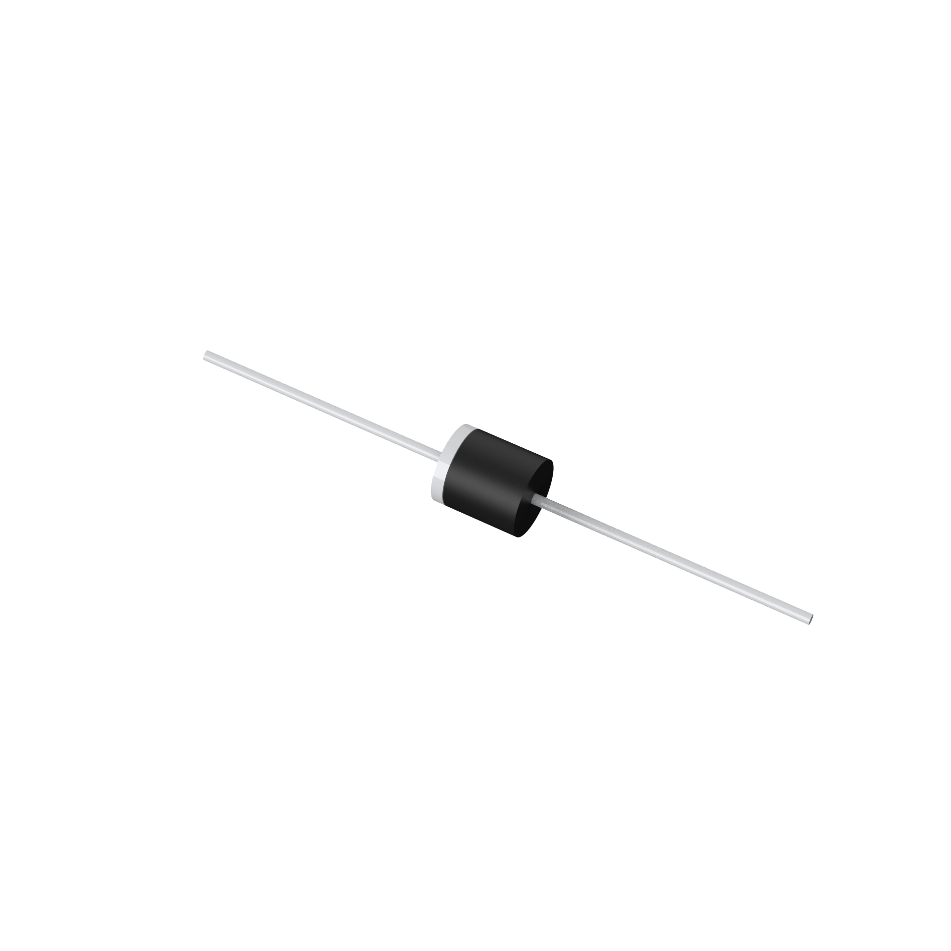
A TVS diode is primarily used to protect equipment from transient events, particularly ESD-related spikes. TVS diodes are often confused with Zener or Schottky diodes, but they are distinct. Composed of a pn-junction semiconductor, a TVS diode conducts during transient voltage peaks. In normal conditions, it remains in high impedance with minimal leakage current. Once the transient voltage exceeds the breakdown threshold, avalanche breakdown occurs, allowing current to pass through the diode, thereby redirecting the excessive current away from sensitive components.
TVS diodes react extremely quickly, often in the picosecond range, making them highly effective in handling fast ESD pulses with rapid rise times.
All TVS diodes function similarly: when a transient voltage spike occurs, it quickly exceeds the diode’s reverse breakdown voltage, causing it to conduct. However, not all TVS diodes are the same, and choosing the wrong protection can result in ineffective transient protection. When selecting a TVS diode, consider the following key parameters:
Reverse Breakdown Voltage (VB): The voltage at which the TVS diode begins to conduct.
Clamping Voltage (VC): The voltage at which the TVS diode significantly conducts and clamps the transient. Lower clamping voltage provides better protection.
Working Reverse Voltage (VWM): The maximum reverse bias voltage under which the TVS diode remains non-conductive, exhibiting high impedance and minimal leakage current.
Peak Pulse Power (PPP): The amount of power the TVS diode can safely dissipate during a transient event.
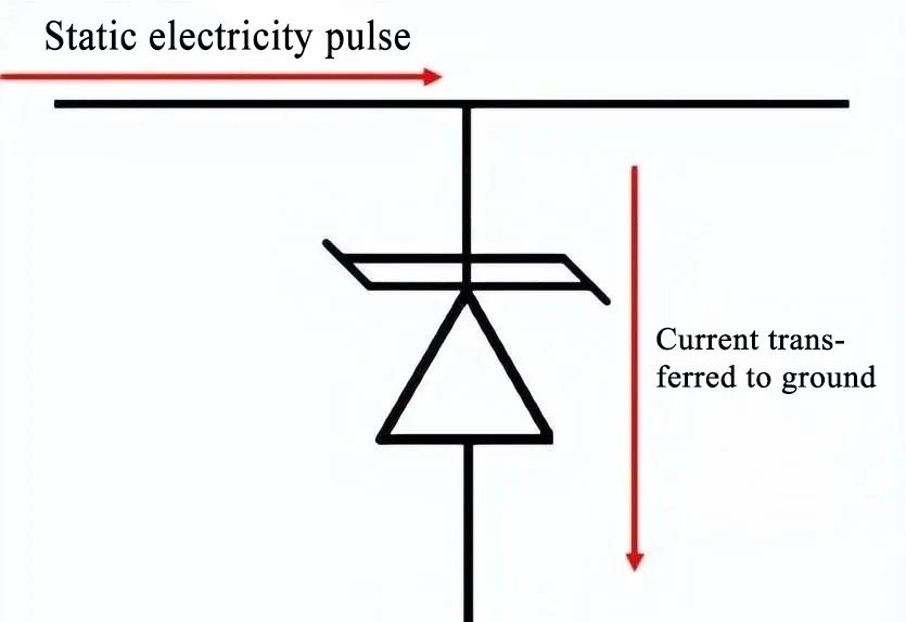
The principle behind TVS diode operation is simple: when the circuit receives an ESD pulse, it rapidly exceeds the diode’s reverse breakdown voltage. Exposed conductors, such as those connected to external connectors, are prone to ESD pulses. If these conductors carry signals to components, the ESD pulse may transfer a high voltage/current to the component, potentially damaging it.
In the presence of a TVS diode, the pulse is diverted through the diode, which provides a low-impedance path to ground. Typically, the anode is grounded, allowing the ESD pulse to discharge to the ground plane, as long as a low-impedance grounding path is available.
TVS diodes come in two types: bidirectional and unidirectional, which serve different purposes:
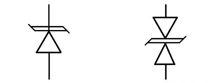
Bidirectional TVS Diodes are used when the circuit carries both positive and negative signals, such as in differential pairs or bidirectional oscillating analog circuits. These diodes offer comprehensive ESD protection, including during grounding faults.
Unidirectional TVS Diodes provide protection when only a single polarity is involved. While these diodes offer protection for typical circuits, grounding faults may expose components to some voltage.
Beyond selecting the right TVS diode, the effectiveness of protection largely depends on the PCB layout itself. The following guidelines help ensure optimal TVS diode performance:
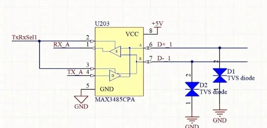
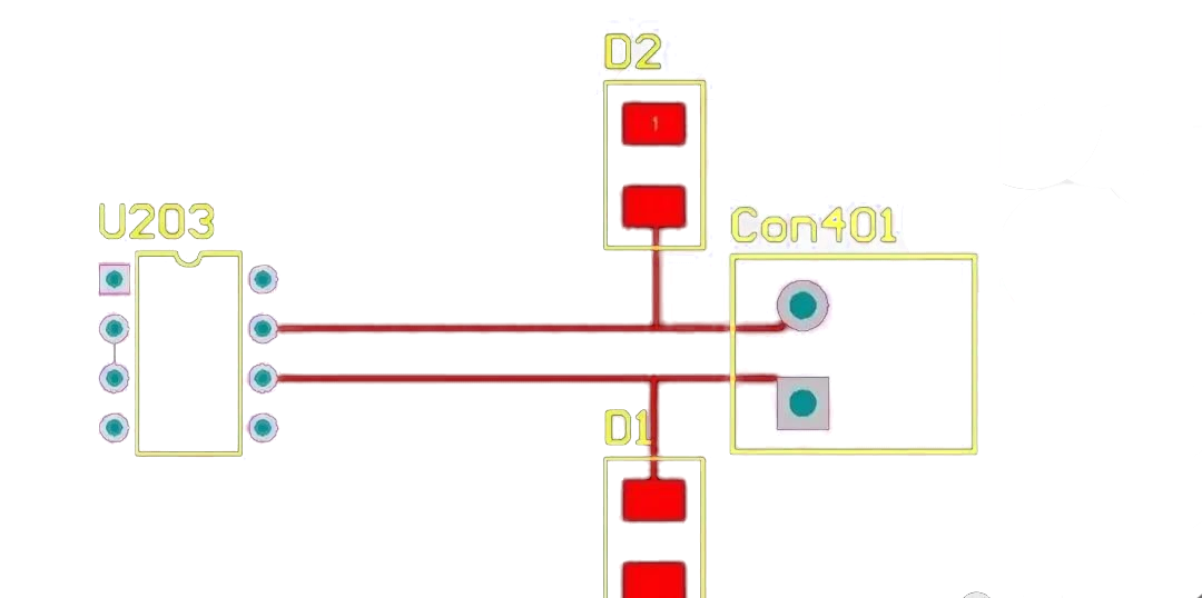
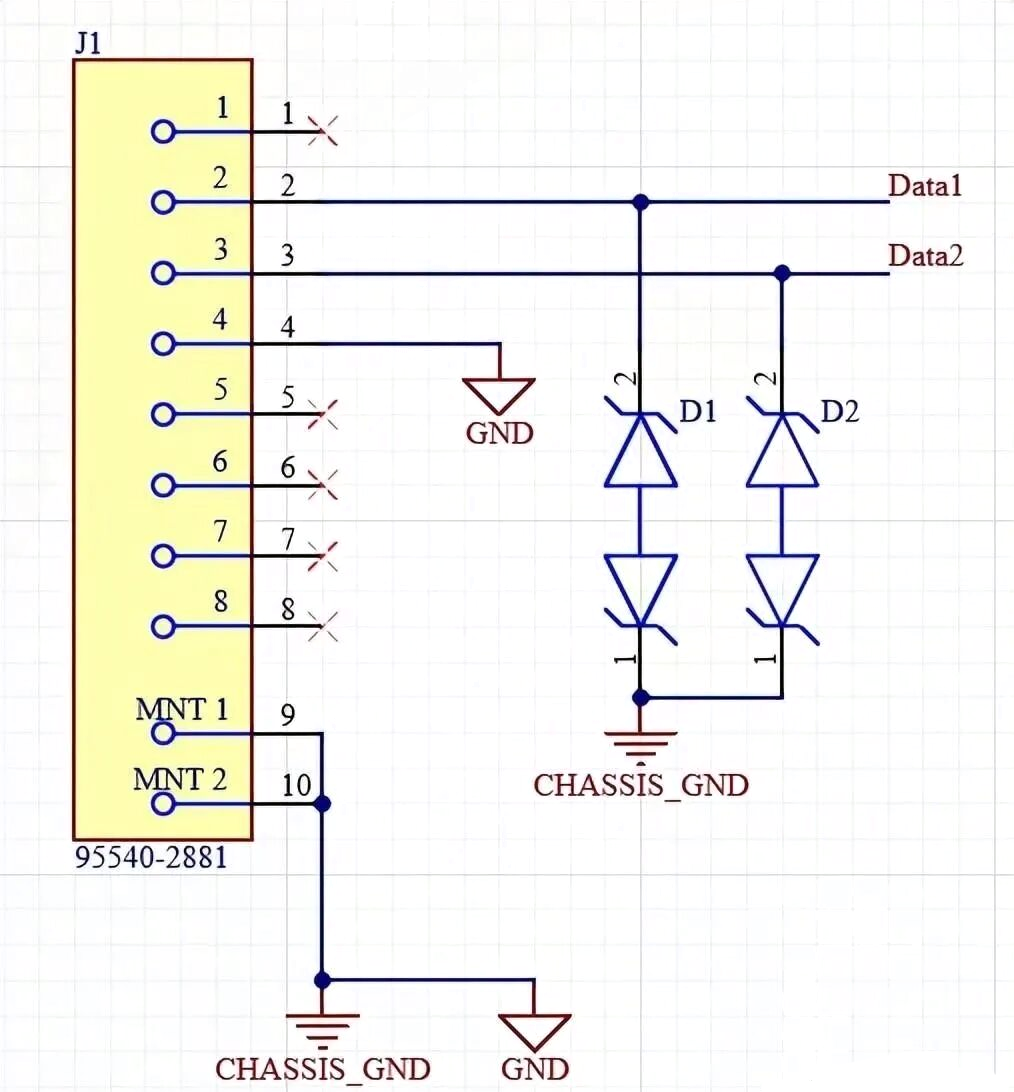
Placement: TVS diodes should be placed near exposed conductors that may be subjected to ESD events, such as connectors or open signal lines. Minimizing the trace length between the TVS diode and the exposed conductors reduces parasitic inductance and improves response time.
Grounding: Ideally, TVS diodes should be connected to a ground plane separate from the protected component’s ground. If not possible, connect to the chassis ground using traces to metal elements like screws or mounting holes. A low-impedance ground is essential for quick dissipation of transient energy.
Eliminating Passive Shielding: Some components, like shielded connectors, are designed to prevent ESD and noise interference. These should be used in conjunction with TVS diodes to ensure full protection. The shield of a connector should be grounded directly to the chassis or ground plane to maintain a low-impedance path for the transient current.
By following these guidelines, TVS diodes can be optimally utilized for efficient surge and ESD protection in circuit designs.
TVS diode protection | PCB layout tips | ESD surge protection | transient voltage protection | TVS diode application | protecting electronic components | TVS diode placement | surge protection design | PCB component protection | TVS diode breakdown voltage