This technical article deeply analyzes the application mechanisms and selection logic of TVS diodes in high-speed signal, power interface, and industrial surge environments, covering typical packages and future development trends.
I. ESD and Surge: Invisible Threats in Digital Systems
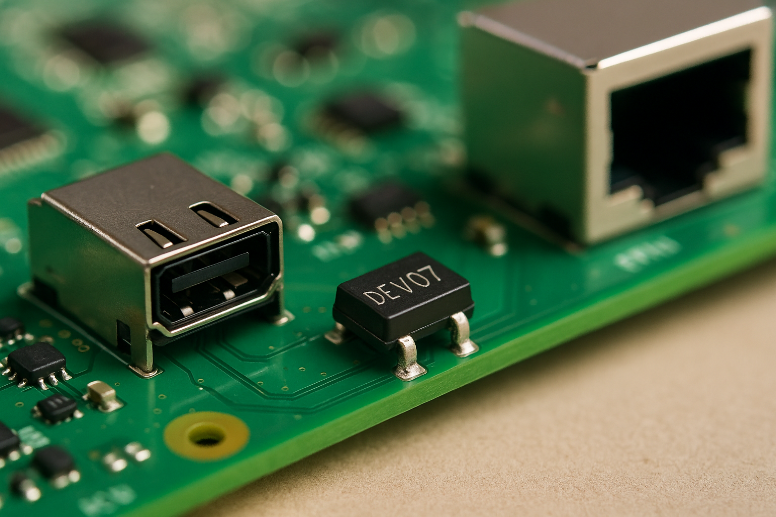
In high-speed digital electronics and power management systems, Electrostatic Discharge (ESD) and transient surge voltages—caused by lightning, inductive switching, or power line anomalies—represent significant yet often overlooked threats. Especially in interfaces like USB, HDMI, CAN, and Ethernet, millisecond-scale voltage spikes can irreversibly damage I/O ports, crash main controllers, or force unexpected system resets.
Transient Voltage Suppression (TVS) diodes, designed for ESD and surge mitigation, offer sub-nanosecond response times (<1ns), low clamping voltages, and high transient energy absorption, making them indispensable in designing robust interfaces.
II. Operating Principle and Behavioral Model of TVS Diodes
TVS diodes operate on a breakdown and clamping principle. When the input voltage exceeds the breakdown threshold (VBR), the diode enters a low-impedance conduction mode, redirecting the transient current to ground while clamping the voltage at a safe level (VCLAMP).
The TVS diode can be modeled as a capacitor in parallel with a Zener-like component, delivering ultra-fast response and tolerating high peak pulse currents (IPP in tens of amperes).
III. Typical Applications and Circuit Design Considerations
For high-speed data lines, TVS diodes must feature extremely low junction capacitance (CJ <1pF) to avoid signal degradation. It's essential to choose low-capacitance TVS models and place them close to the connectors.
At DC input stages—for instance, in industrial PLCs, automotive ECUs, or drone ESCs—TVS diodes act as surge absorbers in parallel with the input rail, capable of clamping pulses conforming to ISO 7637 or IEC 61000 standards.
When switching off inductive loads such as motors, relays, or coils, TVS diodes absorb the high reverse voltage generated, protecting switching transistors (MOSFET/IGBT) from avalanche breakdown.
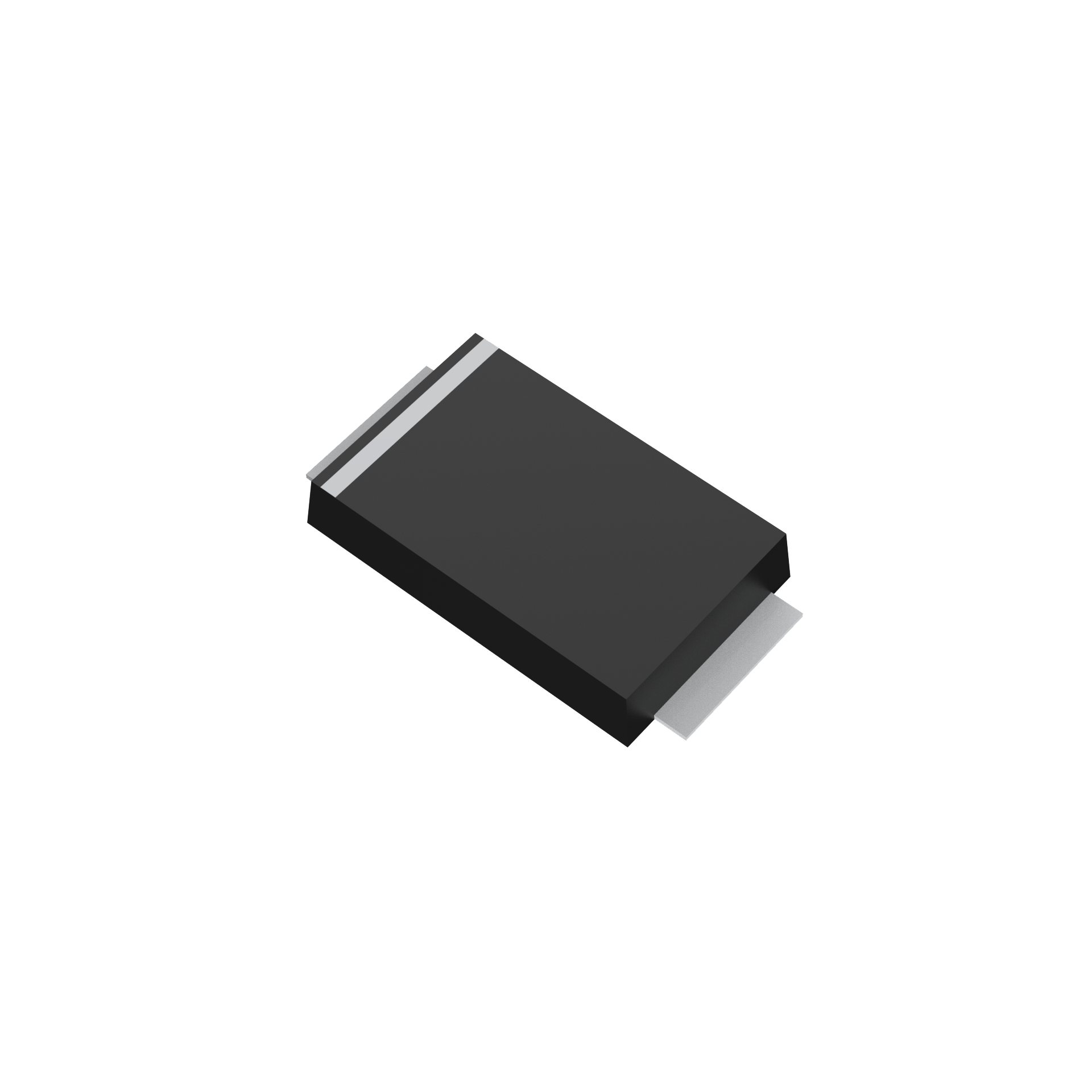
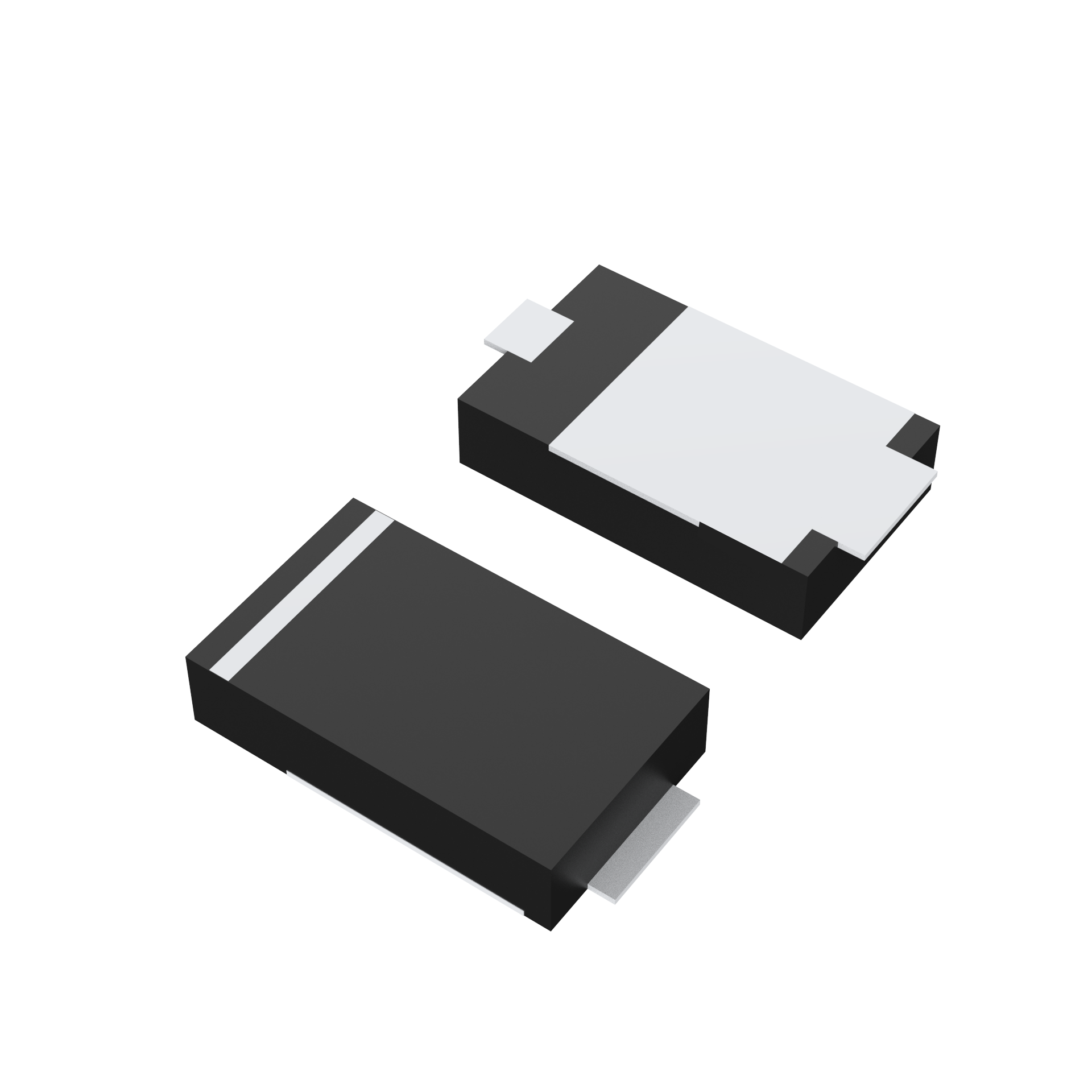
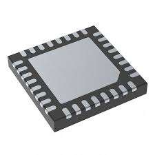
IV. Key Selection Parameters and Package Options
| Parameter | Recommended value/range |
| VRWM (maximum operating voltage) | Should be 10–20% higher than normal operating voltage |
| VBR (breakdown voltage) | Should be lower than the target protection device withstand voltage |
| VCLAMP (clamp voltage) | The lower the better to avoid overvoltage shock |
| IPP (maximum pulse current) | According to standard test (such as 8/20μs) |
| CJ (junction capacitance) | High-speed signal recommendation <1pF |
| Package Type |
SOD-323, SOT-23, SMA, SMB, etc. |
V. Future Trends and Integration Roadmap
Array packaging: Multi-channel USB/HDMI TVS arrays for compact protection;
Bidirectional devices: Suitable for AC signals or bidirectional communication ports;
Embedded integration: Incorporated inside IC packages to save PCB space;
High-power TVS modules: Industrial-grade modules for surge protection in power cabinets or railway systems.
TVS Diodes | Electrostatic Surge Protection | High-Speed Interface ESD Protection