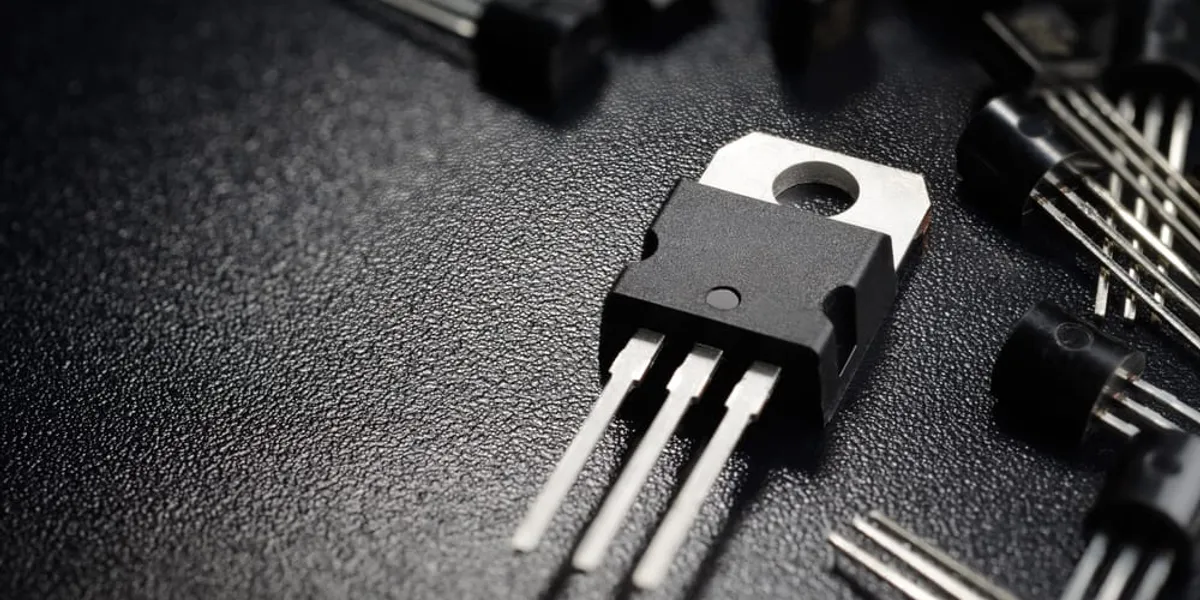
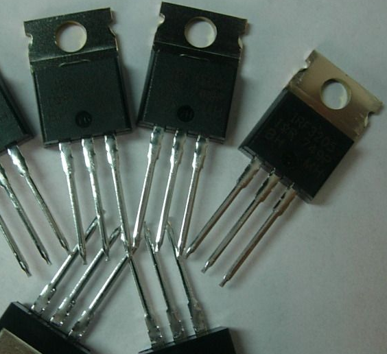
Understanding NPN Transistor Structure and Basic Operation
Definition and fundamental role of NPN transistors in electronics
NPN transistors belong to the family of Bipolar Junction Transistors (BJTs), commonly used as current amplifiers and switches within various electronic circuits. With their three terminals, these components play a vital role in both analog signal amplification tasks and digital switching operations. They're found everywhere from basic power supply designs to sophisticated audio equipment and even in the interface circuits of microcontrollers. The magic happens when a tiny amount of current at the base terminal controls significantly larger currents flowing through the collector. This principle allows for accurate regulation of electrical signals while maintaining efficiency throughout all sorts of electronic applications across different industries.
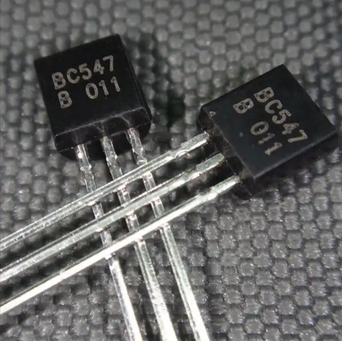
Structure and terminals: base, collector, and emitter
An NPN transistor consists of three doped semiconductor layers:
- Emitter: Heavily doped n-type region that emits electrons
- Base: Thin, lightly doped p-type layer (1–10 µm) that regulates electron flow
- Collector: Larger n-type region designed to collect electrons
This structure forms two pn junctions—the emitter-base and collector-base junctions—each playing a distinct role in operation. During normal use, the emitter-base junction is forward-biased while the collector-base junction remains reverse-biased, allowing controlled electron movement from emitter to collector.
Working principle: electron flow and current control in NPN transistors
Applying a forward bias voltage around 0.7 volts or higher across the base-emitter junction gets things moving, as electrons start flowing from the emitter region into the base area. Now here's what happens next: because the base layer is so thin and lightly doped, most of these electrons don't stick around. Only about 2 to 5 percent actually recombine there to create what we call the base current (IB). The rest, roughly 95 to 98 percent, keep going all the way to the collector side as collector current (IC). What this means for us practically is current amplification. We measure this effect using something called DC current gain, usually represented as beta (β) equals IC divided by IB. Most commercial transistors on the market today have beta values somewhere between 50 and 800, though actual performance can vary depending on specific device characteristics and operating conditions.
Circuit symbol and representation in schematic diagrams
In schematic diagrams, the NPN transistor shows up with an arrow on its emitter that points outward. This indicates how conventional current flows from the base through to the emitter. When building actual circuits, engineers hook up the collector and base terminals to various biasing networks outside the transistor itself. These connections determine exactly where the transistor operates within its range of possibilities. The fact that there's a standard symbol for all NPN transistors really helps when analyzing or designing both analog and digital circuits. Anyone working with electronics quickly learns to recognize this symbol because it appears so frequently in everything from simple amplifiers to complex microprocessor designs.
Operating Modes of NPN Transistors: Cutoff, Active, and Saturation
Cutoff Mode: Transistor as an Open Switch in Digital Circuits
When a transistor operates in cutoff mode, neither the base-emitter nor base-collector junction gets enough forward bias (typically below 0.6 volts), so electrons basically stop flowing from emitter to collector. Think of it as the transistor acting like a closed door between those two points, letting through almost no current at all—sometimes less than one nanoampere. Engineers rely on this state heavily in digital electronics because it effectively turns off the circuit path while consuming next to nothing in terms of power. That's why we see cutoff mode used so frequently in logic gates and other binary systems where low power draw during inactive states is critical.
Active Mode: Linear Amplification and Analog Signal Processing
The active mode comes into play when the base-emitter junction gets forward biased at around 0.7 volts or higher while the collector-base junction remains reverse biased. When operating in this mode, there's a direct relationship between collector current IC and base current IB determined by the transistor's current gain factor beta (or hFE). Most transistors have beta values ranging from about 50 to 300, which creates that nice linear connection needed for proper amplification. This makes them really useful for things like boosting weak signals in audio equipment or preparing sensor outputs before they get processed further down the line.
Saturation Mode: Full Conduction for Efficient Switching
When a transistor reaches saturation, both junctions get forward biased typically around 0.8 volts for VBE and below 0.2 volts for VCE. At this point, the device conducts electricity almost completely. Think of it as acting like a switch that's fully turned on with very little resistance between collector and emitter terminals. The voltage drop here is pretty small, maybe about 200 millivolts give or take. This makes transistors really good at switching things on and off for various components including LED lights, motor controllers, and relay systems. Modern surface mount technology can handle currents well beyond 500 milliamps using these saturated states effectively in circuit boards today.
Voltage and Current Thresholds Defining Each Operating Region
Transitions between modes depend on specific electrical thresholds:
| Parameter | Cutoff | Active | Saturation |
|---|---|---|---|
| VBE | < 0.6 V | 0.6–0.7 V | > 0.7 V |
| VCE | ≈ Supply Voltage | > 0.3 V | < 0.2 V |
| IC/IB Ratio | Near 0 | β (Linear) | < β (Nonlinear) |
These values vary slightly among manufacturers, with studies noting up to ±15% variation in saturation voltages. Designers must account for such tolerances in high-reliability systems through conservative margin planning.
Current Amplification and Key Performance Parameters
Relationship Between Base, Collector, and Emitter Currents (IE = IB + IC)
The total emitter current follows Kirchhoff’s current law: ( I_E = I_B + I_C ). For example, if IB = 1 mA and IC = 100 mA, then IE = 101 mA. Maintaining this balance ensures stable performance in amplifiers and switching circuits, particularly when designing bias networks.
DC Current Gain (β = IC / IB) and Its Importance in Circuit Design
The DC current gain, represented by beta (β), basically tells us how good a transistor is at turning a small base current into a larger collector current. For standard NPN transistors used in everyday circuits, we usually see β values ranging from around 50 up to about 300, though there can be exceptions depending on the manufacturer and application. When β gets higher, it means less current is needed to drive the transistor, which is great news for battery operated devices and other low power systems. But here's the catch: those high gain transistors tend to switch more slowly, making them less ideal for fast signal processing tasks. Real world engineers constantly wrestle with this tradeoff when designing circuits for things like motor controllers where both efficiency and speed matter quite a bit in practice.
Alpha (α = IC / IE) and Its Relationship With Beta (β)
The alpha value, represented by the Greek letter alpha (α), basically tells us what portion of the emitter current actually makes it to the collector side. Mathematically speaking, we calculate it using α equals I sub C divided by I sub E. Now interestingly enough, alpha is connected to beta through another formula: α equals beta divided by (beta plus one). Take for example a common transistor with a beta rating around 100, its corresponding alpha would be approximately 0.99. Why does this matter? Well when designing those complex multi stage amplifier circuits, even tiny efficiency losses at each stage start adding up over time. These cumulative effects can really degrade the quality of signals passing through the system, making proper understanding of alpha parameters absolutely critical for maintaining good signal integrity across multiple stages.
Factors Affecting hFE: Temperature, Manufacturing Variance, and Load Conditions
Several factors influence hFE stability:
- Temperature: A 10°C increase may raise hFE by 5–10%, risking thermal runaway without proper heat dissipation
- Manufacturing tolerance: β can vary by ±30% even within the same production batch
- Load conditions: At high collector currents, hFE may drop by up to 50% due to internal resistance and carrier saturation
Designers mitigate these effects using feedback mechanisms, thermal management practices, and conservative gain assumptions during circuit development.
Common Emitter Configuration and Practical Circuit Applications
Why the common emitter setup dominates amplifier designs
About 70-75% of all analog amplifier circuits actually use the common emitter configuration because it just works so well when balancing voltage gain, current amplification, and those tricky impedance issues. Most single stage CE amps can boost signals anywhere from around 10 times up to maybe 200 times, which beats most other setups hands down. The input impedance typically falls somewhere between 1 and 5 kilohms, making it pretty good at connecting with whatever comes before in the circuit chain. And then there's that output impedance range of roughly 5 to 20 kilohms, which makes these circuits really capable of driving loads effectively. That combination of features explains why engineers keep coming back to CE configurations for things like audio preamps and radio frequency signal processing applications time after time.
Voltage gain and phase inversion characteristics
A key feature of the CE amplifier is its inherent 180° phase inversion: output signals are inverted relative to inputs. This property is valuable in push-pull amplifier topologies for canceling distortion. The voltage gain is approximated by:
Av = - (RC || Rload) / rewhere re ≈ 25 mV / IE is the dynamic emitter resistance. For a 2N3904 biased at 1 mA with a 10 kΩ collector resistor, this yields around 100× voltage gain.
Biasing techniques for stable operation in real-world analog circuits
Stable DC operating points prevent distortion and thermal instability. Common methods include:
- Voltage divider bias: Uses resistors R1 and R2 to establish a fixed base voltage
- Emitter feedback: Incorporates an unbypassed emitter resistor (RE) for improved stability
- DC coupling: Enables direct signal transfer between stages, preserving low-frequency response
Bypass capacitors placed across RE enhance AC gain by shorting the emitter resistor at signal frequencies, boosting performance by up to 40 dB without compromising DC stability.
Case Study: Designing a simple audio preamplifier using an NPN transistor
A practical 2N2222-based audio preamplifier illustrates the CE configuration in action:
| Parameter | Value | Purpose |
|---|---|---|
| VCC | 9V | Supply voltage |
| RC | 4.7 kΩ | Sets voltage gain and Q-point |
| RE | 1 kΩ | Stabilizes DC operating point |
| Cin | 10 μF | Blocks DC from input source |
This circuit achieves 46 dB gain across the full audio spectrum (20 Hz — 20 kHz) with less than 1% THD at 1Vpp input, demonstrating the versatility and reliability of NPN transistors in analog signal processing.
NPN Transistors in Modern Electronics: Switches, Amplifiers, and Future Trends
NPN Transistors as Switches: Driving LEDs, Relays, and Digital Loads
NPN transistors work great as electronic switches that let low power controllers such as microcontrollers handle bigger stuff like LEDs, relays, and motors. When these transistors operate in saturation mode, they basically function as gates controlled by current. Just a tiny amount of current at the base can turn them fully on, so something running on 5 volts can actually control circuits operating at 12 volts. Getting the right value for the base resistor is important because it keeps things working reliably while also safeguarding whatever provides the control signal. That's why engineers keep turning to NPN transistors for all sorts of automation tasks and embedded system designs across industries from manufacturing plants to home automation projects.
Amplification Applications: Boosting Audio and RF Signals
NPN transistors work really well at boosting weak signals in analog circuits because they maintain good linearity while adding minimal noise. These components typically offer decent current gain values above 200 which is why engineers often choose them when dealing with fragile signals in things like audio preamps or radio frequency receivers where signal integrity matters most. High end audio gear frequently employs what's called push pull setups that mix both NPN and PNP transistors together. This combination results in outstanding sound quality with distortion levels that stay under half a percent total harmonic distortion, making these designs popular among audiophiles who demand crystal clear reproduction from their equipment.
BJT vs. MOSFET: Comparing Switching Speed and Power Efficiency
While MOSFETs dominate high-speed and high-power switching (>100 MHz, >10W), NPN BJTs remain relevant in cost-sensitive and linear applications. Key differences include:
| Parameter | NPN Transistor | Power MOSFET |
|---|---|---|
| Switching Speed | 10–100 MHz | 50–500 MHz |
| Control Type | Current-driven (IB) | Voltage-driven (VGS) |
| Cost | $0.02–$0.50 | $0.10–$5.00 |
BJTs are preferred in sub-watt analog circuits and legacy systems, whereas MOSFETs excel in high-efficiency digital power conversion.
Integration in ICs, Logic Gates, and Future Outlook Amid FET Dominance
While CMOS tech has taken over most of today's microelectronics landscape, NPN transistors still play a key role in TTL logic families and those mixed signal ICs we see everywhere. The fact that they work well with 5 volt logic means these old reliable components keep showing up in car electronics and factory control systems across industries. Something interesting is happening though with new silicon germanium versions of NPN transistors. These newer models can handle radio frequency stuff all the way up to around 40 gigahertz frequencies. That opens doors where gallium arsenide field effect transistors used to rule supreme, especially in building out 5G networks and other high speed data transmission equipment.
FAQ
What is an NPN transistor used for?
An NPN transistor is used in electronic circuits as a current amplifier and switch, making it essential for signal regulation and switching activities in both analog and digital applications.
How does current flow in an NPN transistor?
Current in an NPN transistor flows from the emitter through the base to the collector. The base current controls the larger collector current, resulting in amplification.
What are the three operating modes of an NPN transistor?
An NPN transistor operates in three modes: cutoff (no conduction), active (linear amplification), and saturation (full conduction), each defined by specific voltage and current thresholds.
Table of Contents
- Understanding NPN Transistor Structure and Basic Operation
- Operating Modes of NPN Transistors: Cutoff, Active, and Saturation
- Current Amplification and Key Performance Parameters
- Common Emitter Configuration and Practical Circuit Applications
- NPN Transistors in Modern Electronics: Switches, Amplifiers, and Future Trends