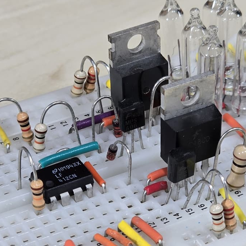
Understanding NPN Transistor Structure and Operating Principles
Layered Semiconductor Structure: Emitter, Base, and Collector Composition
An NPN transistor basically has three layers of semiconductor material arranged in an N-P-N pattern. The outer parts called emitters and collectors are crafted from N-type silicon that's been treated to create extra electrons floating around. The middle section, known as the base, is much thinner and made of P-type material which naturally has fewer electrons (these gaps are what we call holes). These layers form two important junctions between the different materials that let us control electric current flow through the device. Engineers design the base layer to be super thin, usually under about 0.1 micrometers thick, so that electrons don't get lost when they pass through. This thinness helps improve how well the transistor can amplify signals, making it work better in electronic circuits.
| Layer | Material Type | Doping Concentration | Primary Function |
|---|---|---|---|
| Emitter | N-type | High (1019 cm³) | Inject charge carriers into base |
| Base | P-type | Low (1017 cm³) | Controls carrier transit |
| Collector | N-type | Moderate (1015 cm³) | Collects majority carriers |
Electron Flow and Current Control: How NPN Transistors Enable Conduction
When operating in forward active mode, applying around 0.7 volts between the base and emitter gets those electrons flowing from the emitter right into the base area. The base itself is really thin and not heavily doped, so most of these electrons just keep moving through to the collector instead of hanging around to recombine. In fact, only about 5 percent or so actually do recombine in today's better designed transistors. What this means for us practically speaking is current amplification happens because the collector current follows the formula Ic equals beta times Ib. Beta here refers to what we call current gain, and it usually falls somewhere between 50 and 300 depending on the specific transistor design and conditions.
Biasing Requirements for Active, Cutoff, and Saturation Modes
The operational state of an NPN transistor depends on its biasing conditions:
- Active Mode (Amplification): Vbe ≈ 0.7V, Vce > 0.2V
- Cutoff (Off State): Vbe < 0.5V, Ic < 1μA
- Saturation (Switching): Vbe > 0.7V, Vce < 0.2V
Properly biased NPN transistors can transition between states in under 10ns, making them suitable for both analog amplification and digital switching. Maintaining junction temperatures below 150°C through effective heatsinking ensures reliable performance in power applications.
Amplification Capabilities and Performance Metrics of NPN Transistors
Signal Amplification in Analog Circuits Using NPN Transistors
The NPN transistor finds its place all over analog circuitry when it comes to boosting those faint signals. Why? Because they pack quite a punch with their current gain capabilities plus electrons zip through them pretty quickly. Take a look at common emitter setups where tiny changes in base current can actually drive collector currents way higher - sometimes between fifty to three hundred times bigger! That means voltage amplification factors can reach around two hundred times what was originally there. The speed factor is another big plus point for NPNs making them go-to components in RF communications gear and various sensor connections where both bandwidth and clear signal transmission matter most. Most engineers will tell anyone who asks that NPNs beat out PNP alternatives in these applications simply because electrons move faster than holes do inside semiconductor materials, which translates into better performance overall for many electronic designs today.
Current Gain (hfe) and Voltage Gain (Av): Key Amplification Parameters
Two key parameters define amplification performance:
| Parameter | Formula | Typical Range | Design Impact |
|---|---|---|---|
| hfe (β²) | IC/IB | 50–300 | Determines bias stability |
| Av | Vout/Vin ≈ RC/RE | 50–200 (common emitter) | Sets stage gain requirements |
Higher hfe reduces input drive requirements but increases sensitivity to thermal drift. Voltage gain is primarily determined by external resistor ratios, so proper impedance matching is crucial to avoid distortion under load.
Evaluating Switching Speed, Saturation Voltage, and Linearity
- Switching Speed: Transition frequencies range from 2–250 MHz, influenced by base doping and collector capacitance
- Saturation Voltage (VCE(sat)): Typically 0.1–0.3V; lower values improve efficiency in switched-mode power supplies
- Linearity: Total Harmonic Distortion remains ≈±1% in class-A amplifiers when operating within 20–80% of maximum collector current
These characteristics make NPN transistors well-suited for mixed-signal applications such as PWM drivers and multi-stage amplifiers.
Common Emitter Configuration: High Gain and Practical Circuit Design
Why the common emitter setup dominates amplifier designs
Among all amplifier configurations, the common emitter setup stands out as the go-to choice for most applications because it delivers impressive voltage gains ranging from about 40 to 60 dB, along with solid current gains where hfe values often exceed 200 in today's components. What makes this configuration particularly useful is the 180 degree phase inversion it creates, something that works really well when implementing negative feedback in systems with multiple stages. Plus, the input and output impedance characteristics are pretty well matched, making it easy to connect one stage after another without much trouble. Looking at actual industry numbers, around three out of four commercial audio amplifiers on the market today rely on this particular design simply because it performs reliably under almost any kind of signal condition imaginable.
Effective biasing methods: Voltage divider vs. fixed bias stability
Two primary biasing approaches are used in practice:
| Method | Stability (ΔIc/10°C) | Voltage Gain | Best Application |
|---|---|---|---|
| Voltage Divider | ±2% | 55 dB | Precision audio systems |
| Fixed Bias | ±15% | 60 dB | Temporary test circuits |
Voltage divider biasing is preferred in production environments (used in 92% of amplifier designs) because it inherently stabilizes the operating point—a typical 3:1 resistor ratio limits Q-point drift to less than 5% over industrial temperature ranges.
Balancing gain, thermal stability, and signal fidelity
Getting good results means finding the right balance between different design elements. When engineers add a 3.3k ohm emitter degeneration resistor to their circuits, they typically see around a 40% improvement in thermal stability while still keeping most of the voltage gain at about 48 dB. This has been confirmed through various amplifier tests over the years. For those concerned about high frequency response, bypassing that same resistor with a capacitor somewhere between 10 and 100 microfarads can bring back 6 to 8 dB of lost gain without messing up the DC stability. Many designers find this method works well for audio equipment where total harmonic distortion plus noise stays under 0.08%, which is pretty much what audiophiles expect from quality sound systems these days.
Switching Applications in Digital and Power Electronics
NPN Transistors as Switches in Logic Gates and Microcontroller Interfaces
NPN transistors work really well as switches because they can switch quickly between their cutoff state (which is basically OFF) and saturation state (fully ON). These little components play a big role in digital logic gates like AND or OR circuits where they direct electrical signals depending on what inputs are present. The real magic happens when connecting microcontrollers to things that need more power, such as relays or electric motors. Here, NPN transistors act like current buffers, creating a protective barrier between delicate control circuits and those pesky inductive loads or devices that draw lots of current. This protection helps prevent damage to the control system while still allowing it to manage larger electrical demands safely.
Role in TTL Circuits and Digital Switching Networks
Transistor-Transistor Logic (TTL) relies on NPN transistors for their fast switching—under 10 ns—and compatibility with standard logic levels (3.3V–5V). The 0.7V base-emitter threshold aligns naturally with TTL signaling, enabling efficient propagation through multiple logic stages with minimal power dissipation.
Use in Power Regulation and Driver Circuits for Loads
When it comes to power electronics work, NPN transistors can handle pretty hefty loads around the 60 amp range as long as there are proper heatsinks attached. These components find their way into motor driver circuits where they allow for fine control over both speed and torque through PWM techniques that operate at impressive frequencies sometimes hitting 200 kilohertz. For engineers working on tough projects, picking parts with good current gain characteristics and minimal saturation voltage makes all the difference. It keeps things running efficiently while preventing overheating issues even under harsh operating conditions that many industrial systems face daily.
Advantages and Selection Criteria for NPN Transistors in Modern Design
Superior Electron Mobility and Speed Compared to PNP Transistors
In NPN transistors, electrons serve as the main charge carriers and these actually travel faster through silicon material than do the holes found in PNP types. Because of this difference, we typically see around 80% faster switching times with NPN models, which explains why they work so well in those high frequency amplifier setups and digital circuitry applications. Research indicates that when looking at TTL configurations specifically, NPN versions tend to have about four and a half times less signal delay than similar PNP devices. That's one reason why engineers often go with NPN for any design where timing matters most.
Cost-Effectiveness, Availability, and Compatibility With Positive Voltage Systems
NPN transistors dominate the market as the go-to bipolar transistor choice for many applications. They typically cost around 40 percent less than their PNP counterparts and come in all sorts of current ratings from as low as 10 mA right up to 50 A. What makes them so popular? Well, they work great with positive ground systems which is why about three quarters of today's electronics designs incorporate them without much hassle. Most engineers will tell anyone who'll listen that NPNs make life easier when connecting to microcontrollers because there's no need for extra circuits to shift voltage levels or invert signals, something that saves both time and money on the production line.
Key Selection Parameters: hfe, Vce(max), Ic(max), and Thermal Considerations
To ensure optimal performance, designers should evaluate the following specifications:
- Current gain (hfe): Choose ≥100 for amplification stages to maintain sufficient drive sensitivity
- Collector-emitter voltage (Vce(max)): Select a rating exceeding the circuit’s supply voltage by at least 30%
- Current rating (Ic(max)): Include a 20% safety margin above expected peak loads
- Thermal resistance: Maintain junction temperature below 125°C using appropriate heatsinking
For switching applications, prioritize transistors with VCE(sat) < 0.3V and transition frequencies above 100 MHz to minimize conduction and switching losses. Manufacturer-provided thermal derating curves are essential for reliable operation in elevated ambient temperatures.
FAQ
What is the basic structure of an NPN transistor?
An NPN transistor is structured with three layers of semiconductor material in an N-P-N arrangement.
How does an NPN transistor amplify signals?
It amplifies signals by increasing the current at the collector side, driven by the base current multiplied by the current gain (β).
What are the key modes of operation for an NPN transistor?
They include the active mode, cutoff mode (off state), and saturation mode (switching).
Why are NPN transistors favored over PNP transistors in high-frequency applications?
NPN transistors offer superior electron mobility and faster switching times compared to PNP transistors.
Table of Contents
- Understanding NPN Transistor Structure and Operating Principles
- Amplification Capabilities and Performance Metrics of NPN Transistors
- Common Emitter Configuration: High Gain and Practical Circuit Design
- Switching Applications in Digital and Power Electronics
- Advantages and Selection Criteria for NPN Transistors in Modern Design