This article provides an in-depth analysis of the role of TVS diodes in communication device interface protection, including selection parameters and PCB layout recommendations, covering common scenarios such as RJ45, USB, and CAN.
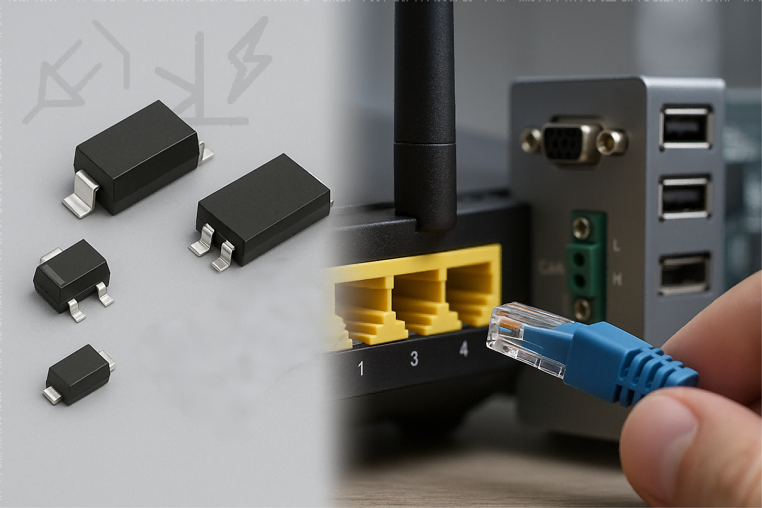
In high-speed communication equipment such as routers, base stations, and Ethernet switches, data ports like RJ45, USB, HDMI, and CAN are exposed to user interaction or external cabling. These interfaces are particularly prone to transient disturbances caused by lightning-induced surges, hot-plugging, or electrostatic discharge (ESD).
While brief in duration (nanoseconds to microseconds), transient voltages often have steep rise times and high peak amplitudes, capable of destroying sensitive PHY chips, microcontroller interfaces, or even vaporizing PCB traces if left unprotected.
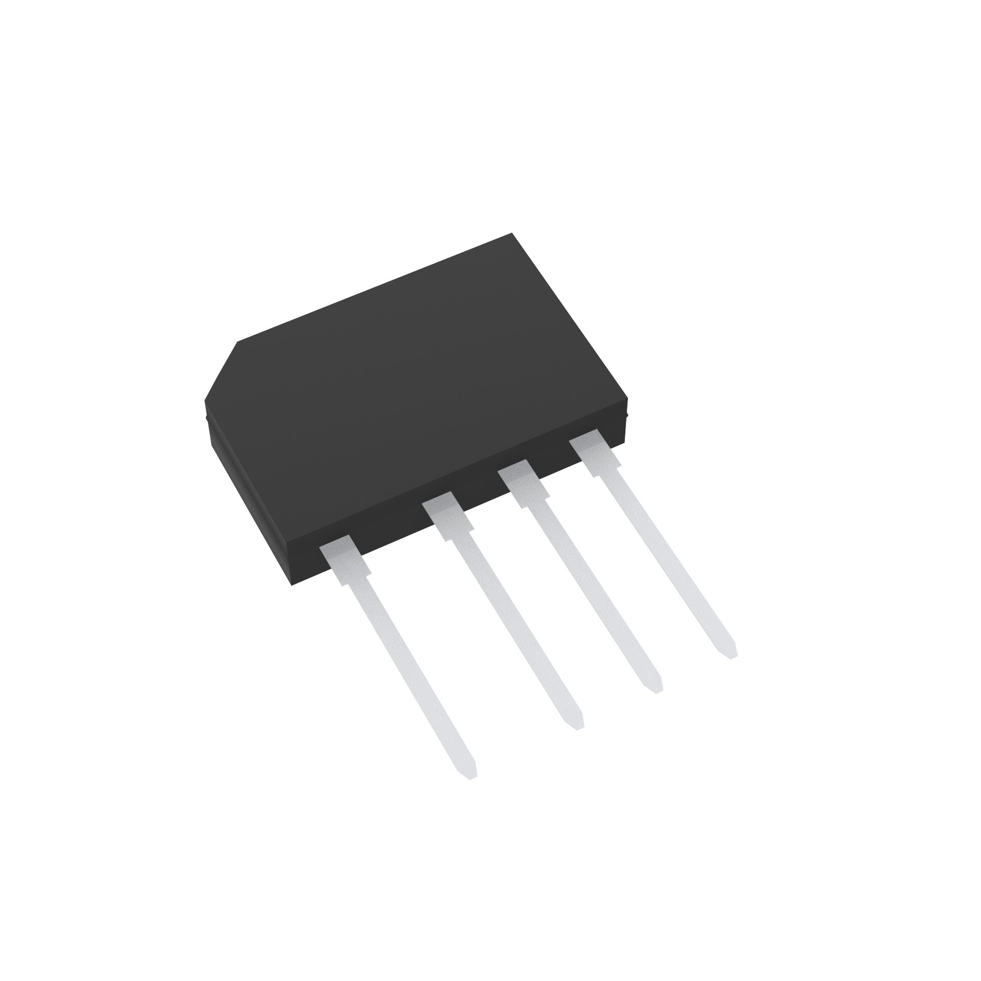
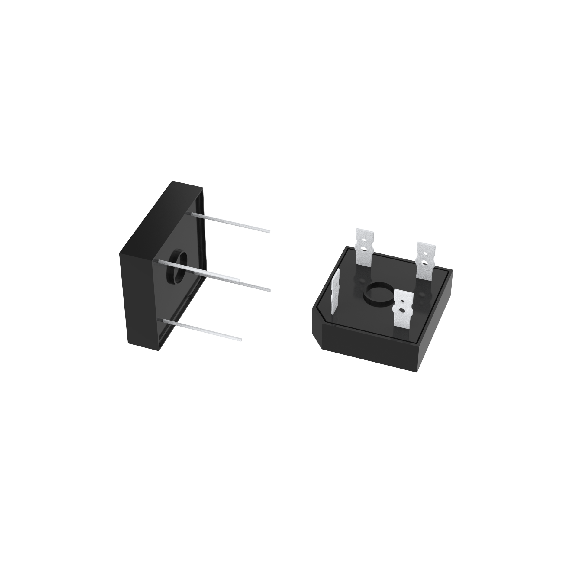
TVS (Transient Voltage Suppression) diodes are semiconductor protection devices designed to clamp transient voltages to safe levels within nanoseconds. They feature ultra-fast response times (<1ns), low capacitance, and tightly controlled clamping voltages.
In communication systems, TVS diodes are commonly used for protecting the following types of interfaces:
RJ45 Ethernet Ports: For lightning-induced surges and common/differential mode transients
USB / HDMI: For ESD and hot-swap events
CAN / RS485: To suppress reverse inductive voltages in long-distance wired systems
Selecting a suitable TVS diode requires matching the interface's electrical characteristics and protection requirements. Key parameters include
|
Parameter |
Description |
Recommended Range |
|
VRWM |
Reverse working voltage |
≥ interface operating voltage |
|
VCLAMP |
Clamping voltage |
< max tolerance of the IC |
|
CJ |
Capacitance |
Few pF to tens of pF depending on data rate |
|
IPP |
Peak pulse current |
Based on expected surge class (e.g. IEC 61000-4-5) |
|
tR |
Response time |
Less than 1ns preferred |
IV. PCB Layout Tips for Effective TVS Deployment
Even with a high-quality TVS diode, poor PCB layout can undermine protection. Key layout guidelines include:
Place TVS diode as close as possible to the external connector
Keep traces short and avoid routing over high-speed signal paths
Ensure low-impedance ground return paths, use stitching vias liberally
With data rates exceeding 10Gbps, traditional TVS designs face trade-offs between protection and signal integrity. Key future directions include:
Ultra-low capacitance TVS (<0.5pF) for high-speed differential signals
Multi-channel TVS arrays to protect multi-wire interfaces like USB/HDMI
Hybrid protection devices with built-in EMI filtering are gaining popularity
TVS Diodes | Interface Protection | Anti-Electrostatic Surge | Communication Protection Solutions